The figure shows the block diagram of complete communication system, which can be divided into three main sections; namely a master unit, remote unit and signal transmission through free space optics. The remote unit is used to control the master unit. The hierarchy of operation is as follows:
1) For Remote Module.
DTMF Keypad will provide control signal to DTMF Encoder.
DTMF Encoder generates the tone frequency signal.
IR Transmitter converts the above into a light signal.
2) Free Space Optics
IR Signal generated by IR transmitter to Master Unit through Free space
IR Receiver reads the light signal and converts it into the tone frequency signal.
DTMF to BCD decoder convert the above signal to BCD
De-multiplexer provides control signal for required switching.
Block Diagram of The Project
Overview Of The Block Diagram:
DTMF Keypad Input:
a. The Unit provides the input for the DTMF dual sine wave generation.
b. On pressing a switch, the 2 sine wave frequencies fetched to the DTMF Encoder.
DTMF Encoder:
a. The 2 sine wave signals are combined and a unique dual tone signal for the particular key is generated and made available for further use.
b. The IC used in this is the DTMF Generator IC named UM912141B.
Optical Transmitter:
a. In the optical transmitter, IR transmission is used.
b. The IR signal is generated by the IR transmitter in the form of the tone.
c. Then the signal is converted into light form and then transmitted.
FSO (Free Space Optics):
a. The FSO is the medium for the transmission of the signal.
b. FSO is the line of sight technology that uses LASER and to provide optical bandwidth connection, that can send and receive voice, video and data information on invisible beam of light.
c. FSO technology require light which can be focused by using either LEDs or LASER
Optical Receiver (IR Photo Diode):
a. Optical receiver receives the light from the space optics.
b. Then the light is converted into the tone frequency signal.
DTMF to BCD Decoder and DEMUX:
a. DTMF or Tone dialing is commonly used
b. DTMF is a tone composed of 2 sine waves of given frequency.
c. DTMF standards specify 50ms tone and 50 ms space duration.
d. The HT9170B is a completed DTMF receiver integrating ICs.
Device Controlling Relays:
a. For controlling the device, the SUGAR CUBE relay is used.
b. It consumes relatively less power compared to other relays.
c. It is compact in size and easily available for various current relays.
Sensors:
a. It senses the appropriate changes and accordingly activates the corresponding sugar cube relay (of the sensors) and performs switching.
Why This Project?
Why This Project?
Cost Effectiveness:
Large numbers of wires need to be laid for all applications that require control and for measurement purposes. This method will provide a cost effective means for achieving all this by a single wire. Transmitting different frequency signals through a single wire and then using them for different applications provides the single wire control.
Loss-Less System:
The transmitting of the control signal through the optical fiber in the form of the infrared signal will provide a loss-less system. As the loss in the optical fiber is negligible, the weakening of the signal due to losses does not take place. Also the transmitted signal is not affected by stray signals because the fiber does not allow them to enter its interior.
Central Control:
This project will provide a means of establishing control center, which will monitor all the applications of the industry. Sitting in the control room, a person can keep a check and control all the major operation of an industry.
Remote Operation:
Regardless of the distance of the appliances from the control room, it can be controlled without any problem.
Transmitter Unit :
The Fig below shows the keypad of the transmitter module. The various signals corresponding to the keys pressed are generated through this pad.
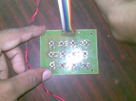
Keypad
The Fig is the transmitter unit which contains the dialer IC UM912141B. this unit transmits the tone generated by the keypad.
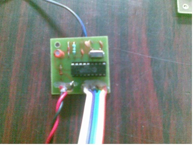
Transmitter Unit
Circuit Diagram Explanation
Explanation of Circuit:
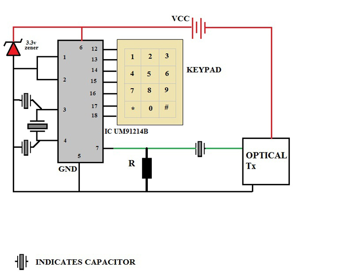
The figure is shown in the circuit diagram tab of transmitter module. Its main parts are DTMF dialer, IC UM91214B and Optical transmitter.
The circuit employs DTMF technique to control ten applications. However it can be modified for multiple applications. A 9 volt b battery is used for remote control circuit. However the DTMF dialer IC requires only 3 Volts for its operations, which is derived with the help of zener diode voltage regulator.
The controller has 7 relays. These are arranged in 4 rows (R1-R4) And 3 columns (C1 to C3) using 7 lines terminating at corresponding inputs of DTMF Encoder UM91214B.IC generates distinct dual tone signals corresponding to the relay triggered .this signal is rooted to receiver through optical fiber.
DTMF Tone Generator UM91214B:
The DTMF encoder IC UM91214B is commonly used as a dialer IC in telephones. Its function is to generate the DTMF tones correspond to the energized relay. Its internal block diagram is shown in figure.
For its time based UM91214B requires a quartz crystal of 3.58 MHz which is connected between pins 3 and 4 of dialer IC to form part of an internal oscillator circuit. The oscillator output is converted into appropriate DTMF signals through frequency division and mixing by controlling logic. Pins 15 to 18 are row pins and pins 12 to14 are column pins.
IC UM91214B also incorporates a 20 digit dialed no. memory. This feature of the IC is not used in the present remote control system. The memory unit and read write pointer logic is controlled by the control logic. The DTMF tones are obtained from the pin 7 of the IC. The IC also has some control inputs that are not used in its present application.
OPTICAL TRANSMITTER & RECEIVER :
Introduction:
This unit generates light signals, which has a wavelength slightly greater than the wavelength of a visible light. These signals are called as infra-red beams.
In the infra-red based remote control system, infra-red transmitter LED is used in the transmitter, optical fiber is used as signal transmission and receiver uses a matching infra-red photo diode or a photo transistor to receive the transmitted infra-red signals. The transmitted signal is invisible to the naked human eye, but an infra-red photo diode sense the signal.
The light we can see as the wavelength from 4×10(-7) m to 7 x 10(-7) m just above and below this visible light spectrum two invisible lights are situated, these UV light and IR light.
RECEIVER UNIT :
The below figure shows the receiver unit.
Receiver Unit
Receiver Circuit Explanation:
The receiver module decodes the received DTMF Signals with the help of DTMF decoder IC HT9170B that provides the binary o/p according to the switch pressed in the remote area. It also provides STD signals that indicates the receipt of valid DTMF code.
Whenever a particular key is pressed in the Remote control Unit, the signal transmitted via free space is received by the DTMF Decoder and it generates the corresponding binary code in its o/p line A, B, C, D (on pin no. 11, 12, 13, 14 ). The delayed steering trigger o/p (STD) also goes high, which becomes low when the key is released.
The binary o/p of DTMF Decoder is connected as input to 4-line to 16-line decoder IC TC4514BP. One of the 16 o/p latches corresponding to the input data goes high as latch enabled (LEN) is kept permanently high, when the control input EN is connected to STD signal, which goes high as long as a switch on the keypad and all o/p lines of this IC remains low. However, when the user release the keypad switch at the remote unit, the transmission of DTMF signal stops and the STD signal o/p goes low to o/p the already latched data. The o/p line of this IC corresponding to release key on the keypad goes high. Thus, a low to high transition occur in one of the decoder o/p lines corresponding to the switch pressed and released in the Remote Unit.
The positive going pulse triggers the corresponding the D-Flip flop which is wired in a toggle Mode to control the desired appliance. Hence, a particular appliance can be turned ON by momentarily pressing the corresponding Key. Subsequently, it can be turned OFF by momentarily pressing the same key again.
Set and Reset keys in the keypad act as a master switches for turning ON and OFF, respectively, all the appliances. When these keys are pressed (one at a time), they generate signal that are decoded by the IC HT9170B as B and C (HEX) respectively. The corresponding o/p lines of IC TC4514BP are connected to set and reset terminal respectively, of all the toggle flip flop, to turn on/off all the appliances simultaneously.
Circuit Explanation Continued
DTMF To BCD Decoder Unit (IC HT9170B):
Description:
The HT9170B is a complete DTMF receiver integrating both the band split filter and digital decoder function. The filter section uses switched capacitor techniques for high and low group filters; the decoder uses digital counting techniques to detect and detect all 16 DTMF tone pairs into a 4 bit word. External component count is minimized by on chip provision of a differential input amplifier, clock oscillator and latch 3 state bus interface[9].
Features:
a. Complete DTMF receiver
b. Low power consumption.
c. Internal gain setting amplifier.
d. Adjustable guard time.
e. Central office quality
f. Power down mode
g. Inhibit mode
Functional Description:
The HT9170B monolithic DTMF receiver offers small size, low power consumption and high performance. Its architecture consists of a band split filter section, which separates the high and low group tones followed by a digital counting section which verifies the frequency and duration of the received tines before passing the corresponding code to the o/p bus.
Filter Section:
Separation of the low group and high group tones is achieved by applying the DTMF signal to the input of the two 6th order switched capacitor band pass filter, the bandwidth of which corresponds to the low and high group frequencies. The filter section also incorporates the notches at 350 and 440 Hz for exceptional tone dialing rejection. Each filter o/p is followed by a single order switched capacitor filter section which smoothes the signals prior to limiting which is performed by high gain comparators, which are provided with hysteresis to prevent detection of low unwanted low level signals. The o/p of the comparators provides full rail logic swings at the frequencies of the incoming DTMF signals.
Decoder Section:
Following the filter section is a decoder employing digital counting techniques to determine the frequencies of the incoming tone and to verify that they correspond to standard DTMF frequencies. A complex averaging algorithm protects against tone simulation by extraneous signals such as voice while providing tolerance to small frequency deviation and variations. This averaging algorithm has been developed to ensure an optimum combination of immunity to talk off and tolerance to the presence of interfering frequencies (3rd tones) and noise. Whether detector recognizes the presence of 2 valid tones (this is referred to as the “signal condition” in some industry specifications) the “early steering” o/p will go to an active state. Any subsequent loss of signal will cause ESt to assume an inactive state .
Steering Circuit:
Basic Steering Circuit.
Before registration of a decoded tone pair, the receiver checks for a valid signal during (referred to as character reorganization condition). This check is performed by an external time RC constant driven by ESt. A Logic high on ESt causes Vc (see above figure) to rise as the capacitor discharges. Provided signal condition is maintained ( ESt remains high) for the validation period (tGTP) , Vc Reaches the threshold( VTSt) of the steering logic to register the tone pair, latching its corresponding 4 bit code into the o/p latch. At this point, the GT o/p is activated and drives Vc to Vdd. GT continues to drive high as long as Est remains high. Finally, after a short delay to allow, the o/p latch to settle, the delayed steering o/p flag, (StD) goes high, signaling that a received tone pair has been registered. The contents of the o/p latch are made available on the 4 bit o/p bus by raising the 3 state control input (TOE) to logic high. The steering circuit works in reverse to validate the intrepidity pause between signals. Thus, as well as rejecting signals too short to be considered valid. The receiver will tolerate signal interruptions (drop out) too short to be considered a valid pause. This facility, together with the capability of selecting the steering time constants externally, allows the designer to tailor performance to meet a wide variety of system requirements.
Applications:
a. Paging systems
b. Repeater systems/mobile radio
c. Credit card systems
d. Remote control
e. Personal computers
f. Telephone answering machine
4-Line To 16- Line Decoder Unit (TC4514BP):
General Description
The TC4514BP and TC4515BP are 4 to 16 line decoders who latched inputs implemented with complementary MOS (CMOS) circuits constructed with n and p channel enhancement mode transistor. These circuits are primarily used in decoding applications where low power dissipation and /or high noise immunity is required. The IC TC4514BP (o/p active high option) presents a logical “1” at the selected o/p, where as the TC4514BP presents a logical “0” at the selected o/p. The input latches are RS type flip flops, which hold the last input data presented prior to strobe transition from “1” to “0”. This input data is decoded and the corresponding o/p is activated. An o/p inhibit line is allowable .
Latch ( HEF4013BP):
Description:
The HEF4013BP is a dual D type flip flop which features independent set direct (SD), clear direct (CD), clock inputs (CP) and Outputs (O,O). Data is accepted when Cp is low and transferred to o/p on the positive going edge of the clock. The active high asynchronous clear direct (CD) and set direct (SD) are independent and override the D and CP inputs. The outputs are buffered for best system performance. Schmitt trigger action in the clock input makes the circuit highly tolerant to slower clock rise and fall times .
Pining:
a. CP clock input (L to H edge triggered).
b. SD asynchronous set direct input (active high).
c. CD asynchronous clear direct input (active high).
d. True o/p.
e. Complement o/p.
Application Information:
a. Counter/ Divider
b. Registers
{ c. Toggle flip flop
Sugar Cube Relay:
This relay is known as the sugar cube relay because its shape is just like the cube of sugar. It is low cost relay for electric appliances.
It consumes relatively less power compared to other relays. It is compact in size and easily available for various current ratings.
It has 5 terminals, 2 for normally closed operations, 2 for normally open operations and 1 common terminal. This sugar cube relay which will act as a switch in the circuit either in normally closed mode or normally open mode. Common terminal will decide whether normally closed or normally open operation will be there.
APPLICATION :
Introduction:
S1 line of the 16 output latched goes high. This output line is connected to the latch, which is dual D-Flip Flop. Thus the relay will operate. As a result of this supply circuit to the motor will be completed and motor will start.
When again the same key is pressed the same output line will receive a logic low due to the latch. Due to this supply circuit to the motor will be incomplete and the motor will stop.
Changing Of Connection Concept
Reverse Operation (Changing Of Connection Concept):
Forward/Reverse Operation of 1-Phase Induction Motor
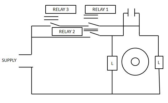
In the above figure relay 1 is closed; relay 2 and 3 is in normally open mode.
When key 2 is pressed, the control signal generated as shown below in block diagram will activate relay 1 and 2. As a result, the motor will operate in reverse direction. When the same key is pressed again the motor will again operate in forward direction. Here relay 3 is provided for the on/off operation of the motor.
As shown in above figure Fig ,when the control relay will be energize by the received signal the normally opened contacts will be closed and motor will start.
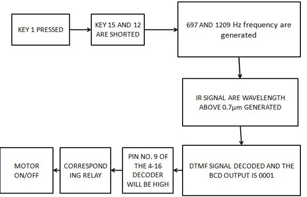
Block diagram for reverse operation
The keypad output is connected to 2 input lines R1 and C1 of the DTMF dialler IC UM91214B. Depending on the BCD code received on the output pins, the corresponding relays will operate and the BCD code will be passed to the DTMF dialler IC. At the output of DTMF dialler IC, an IR led is provided which converts the frequency signals into corresponding light signals of wavelength above 0.7µm. this light signal is then transmitted through free space. The receiver uses a matching IR photodiode or phototransistor to receive the transmitted IR signals
HT9170 is used to convert the received DTMF signal into the BCD code. Separation of the low group and high group is achieved by applying the DTMF to the input of two sixth order switch capacitor band pass filter, the bandwidth of which corresponds to the low and high group frequencies. The binary output of the DTMF decoder is connected as input to 4-16 line decoders CD4514.
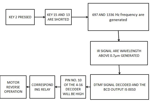
Block diagram Forward/reverse operation
Speed Control (Voltage Variation Concept):
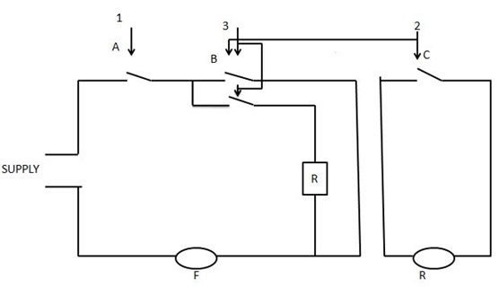
Speed Control Circuit
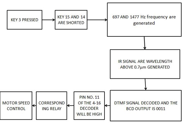
Block Diagram for Speed Control
When the speed control key is pressed, the speed of the motor decreases. And when the same key is pressed again the original speed is restored.
When control signal 1 is provided, relay A which is normally open relay is activated. This results in the start of the motor. Relay B is normally closed relay and relay C is normally open relay. With control signal 2 relay B and c will be activated and the motor will operate in reverse operation.
Relay D is in normally open mode. With control signal 3, relay B will be open and relay D will be closed, resulting in the decreasing in speed. Hence speed control can be provided.
Control of Light:
When the LIGHT key is pressed, it turns on a bulb and pressing it again switches it off. This application in a broad sense can be used to provide central control of light in industries.
A siren operation can be provided which hoots on the press of the key indicating a break., a danger signal etc.
PCB LAYOUT
The PCB layout of the transmitter and receiver is as shown in the figures given below.
Transmitter Part:
Keypad:
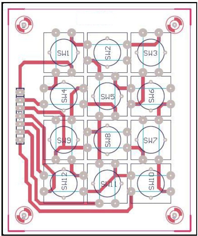
PCB Layout of Keypad
This Layout is the layout of the DTMF keypad that we use for the generation of the Dual Tone Multi Frequency Signals. It contains 12 keys and they are arranged in a matrix form made of 4 rows and 3 columns. For Military purposes, a 4th Column is also used to maintain the privacy.
Transmitter Part:
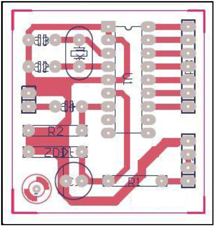
Transmitter Unit
This PCB Contains the main heart of the system and it is the IC UM912141B. This IC is used for the generation of the dual tone signals from the combination of 2 frequencies; one from a lower band the other from the higher band. The output obtained is further sent for the transmission through the fiber optic cable after converting it into light signals.
Receiver Part:
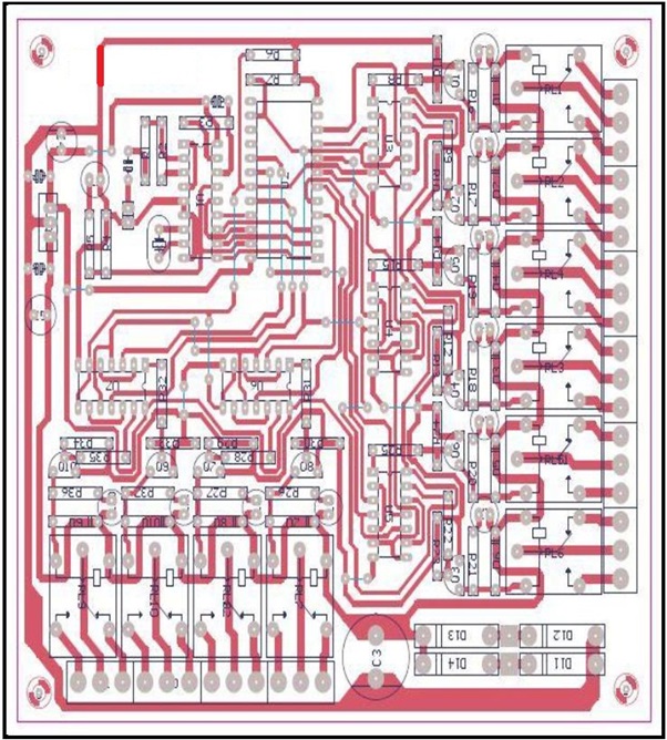
Receiver Unit
Project Application Videos
Project Application Videos
Fire Sensor
Transmitter and Receiver
Vibration Sensor
Project Source Code
Circuit Diagrams
Filed Under: Electronic Projects



Questions related to this article?
👉Ask and discuss on EDAboard.com and Electro-Tech-Online.com forums.
Tell Us What You Think!!
You must be logged in to post a comment.