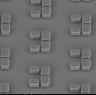
Jacob Martin, in one of his project, has made some milli or microfluidics by using the free space on the template and find out the probability of using laser engraving and cutting for homemade microfluidics for simple lab-on-a-chip applications. The microfluidic devices used in this project is built by using femtosecond laser machining and spectroscopy.
The material used here is acrylic 3mm and two different types of chips are made where one is engraved and other is cut. Install Inkscape, which is an open source vector art drawing program, to set up and to download the template from the website.
After this, two dissimilar etched designs are shaped – a spiral and a shrinking channel. As we proceed, the pictures of the shrinking channel design can be clearly seen with the machined beam profile of 100 microns. This is followed by the screening of the Edge of the chip with 100 microns of melting. Next, the spiral design is shown closed with the overlap of the channels.

Simple laser cut milli-/microfluidics using Ponoko (Image Courtesy: blogger.com)
It is recommended to use straight channels and the distance between the features must not be smaller than 50 microns and 100 microns. For profiling, the surface, the Dektak II from the Microfabrication Facility was used with the shrinking channel. As Dektak runs along the surface to sense the unevenness, the needle runs perpendicular to the course of the laser to quantify the undulations made by the laser.
Next, a laser cut flow cell and the reaction chamber are being cut down and the chips are sandwiched with plastic around them to grip the fluid in the channels. The engraved chips can be used for making chips that mixed liquid or else it can also be used before chemicals go into smaller microfluidic channels as a premier.
Filed Under: Reviews


Questions related to this article?
👉Ask and discuss on Electro-Tech-Online.com and EDAboard.com forums.
Tell Us What You Think!!
You must be logged in to post a comment.