A reliable 5 V supply is at the heart of countless electronic applications, from chargers and adapters to small-scale embedded systems. In this project, we’ll walk through the design of a compact 5 V power supply that operates directly from the AC mains. To achieve this, we’ve chosen a non-isolated topology — a common approach in SMPS, adapters, and low-cost chargers. Because no external transformer is required, one side of the AC line is tied to the DC output ground, meaning the output is not electrically isolated from the mains.
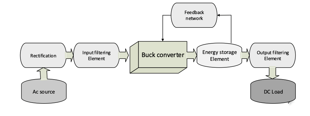
Figure 1. This block diagram is an overview of the non-isolated circuit.
In this topology for the conversion of AC to DC, the Buck converter is needed, which works on a switching topology. The internal MOSFET in the converter IC and oscillator generates the PWM signal and regulates the output voltage through a feedback network. Conceptually, it is the same as a DC to DC buck converter, so before going further, please refer to our previous series on SMPS to know about the working of the buck converter
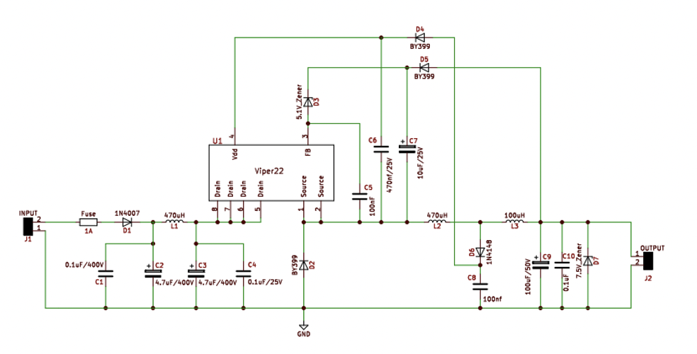
Figure 2. Circuit diagram.
Components needed:
| Name | Specification | Quantity |
| Viper22A | Buck converter | 1 |
| Fuse | 1A | 1 |
| Diode D1 | 1N4007 | 1 |
| Zener diode D3 | 5V/0.5W | 1 |
| Zener diode D7 | 7.5V/0.5W | 1 |
| Zener diode D2,D4,D5 | BY399 | 3 |
| Zener diode D6 | 1N4148 | 1 |
| Capacitor C2, C3 | 4.7uF/400V-electrolyte | 2 |
| Capacitor C9 | 100uF/50V-electrolyte | 1 |
| Capacitor C1,C4,C5,C8,C10 | 0.1uF/25V-ceramic | 5 |
| Capacitor C6 | 470nF/25V-ceramic | 1 |
| Capacitor C7 | 10uF/25V- electrolyte | 1 |
| Inductor L2 | 470uH/1A | 1 |
| Inductor L3 | 100uH/1A | 1 |
Selecting the components
Voltage Regulator
The regulator principle of operation should be of a switching type, as switching regulators are more efficient than linear ones. In switching regulators, we also have the following types of regulators:
- BUCK
- BOOST
- BUCK-BOOST
For this application, we will use the Buck converter IC. The following are the parameters for selecting the IC:
- Built-in MOSFET drain voltage
- Operating power supply voltage
- Output Power
- Support non-isolated design
VIPER22 IC
The Viper22 is a buck converter; it has a MOSFET inside it with a few comparators. Below are the specs of the Viper22A IC:
- Drain voltage – 730V
- Operating power supply voltage — 9V to 38V
- Output Power — 12W
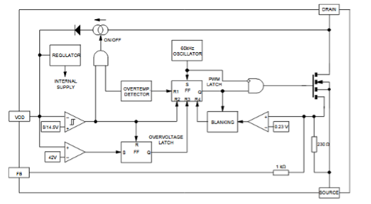
Figure 3. Internal diagram of Viper22 and its pinouts
VDD — The VDD pin of the IC is used to control the power supply of the internal circuit and also to provide the charging current in the initial stage. The comparator compares the VDD voltage. For VDDon = 14.5V, the Viper starts switching, and for VDDoff = 8V, the Viper stops switching.
Drain — MOSFET drain and used by the charging source in the initial stage
SOURCE — MOSFET Source and circuit ground
FB — This controls the maximum drain current limit of the IC
High current protection and rectification
For a high inrush current and short circuit current, a fuse is used at its input side, which will blow when a current greater than 1A.
To convert the AC voltage into DC, a half-wave rectifier is used; the D1 diode provides the half-wave rectification.
Input filtering
Selecting a filtering capacitor
The capacitor minimum voltage should be 1.5times greater than the input AC voltage, and the capacitance is two or three times the output power.
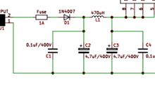
Figure 4. The C2, C3, and L1 form a Pi filter and also reduce the EMI noise. The ceramic C1 and C4 help to reduce the ESR of the electrolyte capacitor.
AC input – 220V then
Voltage rating of Cin = 2*220 = 440V
Output power – Vout*Iout = 5*0.1= 0.5W then
Cin = 2*0.5 = 1uF
As per availability C3, C4 are 4.7uF/400V.
Selecting the VDD capacitor
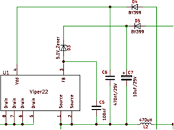
Figure 5.
When the device starts, it will receive some energy from the inductor, so the C6 capacitor helps in filtering and stabilizing the VDD voltage (Figure 5). It will also set the startup time of the IC. The datasheet recommends a 100nF capacitor, but by considering the output voltage, a 470nF/25V capacitor can be used in the circuit.
The C5 capacitor is also responsible for filtering the voltage to the FB pin, and a small ceramic on a pico farad works fine here.
Output diode
The output diode D2 is called a catch or freewheeling diode. In an ON-OFF period of the MOSFET, the inductor passes the energy through a diode to the output. As the diode is switched ON and OFF so a fast rectifying diode is needed which is compatible with the IC frequency. The drop in the diode causes losses in the circuit, which affects the efficiency.
-
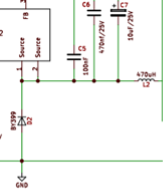
Figure 5.
Low forward voltage drop
- Rated reverse voltage of diode > Vin
Vin (DC) = 220*1.414= 320V
i.e Vfr > 320V on the safe side 400V can be used.
We have used BY399 diode in the circuit.
Calculating losses in BY399 diode
Pd = Forward voltage drop *Iout
Pd = 1 *0.1
Pd = 0.1V
Selecting Inductor
The inductors L2 and L1 are a function of VDD; the ratio of L2/L1 is decided by the input AC line. For 200-265V AC, a 3-4 ratio is suitable with a low ESR inductor (Figure 6).
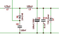
Figure 6.
Here L2 – 470uH
L3 – 100uH
The ratio is 4.7, and it works fine in our design
The inductor output helps in determining the discontinuous and continuous modes of operation. In continuous mode, the losses are more compared to discontinuous mode. To know more about continuous and discontinuous modes, please refer to our previous series of SMPS.
The equation below sets the inductor boundary condition for continuous and discontinuous modes. For operating in the discontinuous mode, the L should be lower than this
L = 0.5*R*(1-D)/f
R = output load, 50E
f = frequency of the IC, 60kHz
D = duty cycle, Vo/Vin= 5/320= 0.0375
L = 410uH(approx.)
We have used L2 = 470H and L3 = 100uH
Selecting a zener diode and other diodes
The zener diode D7 at the output is used to clamp the output voltage in a no-load condition. The buck converter gives a peak voltage in a no-load state. A Zener diode with an output voltage higher than 3-4V is recommended.
The D4 and D5 can be standard diodes, and D3 should have the same voltage rating as the output, i.e, 5V.
Output capacitor
The C8 capacitor provides the current to the Viper and then transfers it to C6. The energy stored by the inductor will depend on the inductor. C6 with 80-100nF with a voltage rating given by the inductor ratio should be selected.
The output C9 capacitor, along with the C10 ceramic, keeps the output ripple low. We can use a 47uF to 220uF capacitor for C9.
Circuit working
Drain voltage — The voltage from the C3 capacitor is delivered to the Drain of the IC from pin 5 to 8.
OFF state — When the first-time circuit starts, the Viper is not switching, and the internal current source in the IC supplies 1mA to the VDD pin; this current charges the C6. When VDD reaches 14.5V, then the current sources turn off and Viper starts switching.
In this period, the output energy is supplied by the inductor and output capacitor, which are charged in the previous state (ON state).
ON state — During this period, Viper is switching and the stored energy in the C6is supplied to the output, thus energy stored in C6must be greater than the energy needed for output current plus energy to charge the output capacitor before VDD falls below 8V. Therefore, the charging and discharging time of C6will decide the ON and OFF time of the circuit.
During this state, the inductor also charges through the internal MOSFET, and energy is being supplied by the C6 to the output
Freewheeling state —This state comes along with the OFF state, when the VDD voltage falls below 8V after supplying all the energy to the output, then Viper stops switching (OFF state). Now again the current source turns ON and simultaneously the inductor starts discharging through diode D2 (forward biased).
Output regulation — The output voltage is regulated by D3, D5, and C7. During the freewheeling state, the D5 charges the C7, and the D4 charges the C6. During this time, the source or ground reference is one diode drop; this will compensate for the energy in C7 and C6.
The output voltage is the same as the Zener D3 voltage. The D3 zener is a low-current zener that gives the best accuracy of the output voltage.
Thermal management
For heat management of the IC, please refer to our article on heatsink selection.
Practical observation
Vin = 220V AC, Tested in a closed box, no natural convection.
No load, Vout = 7.23V
| Voltage(V)
(Output) |
Current(A)
(Output) |
IC case Temperature
(deg) |
Time
(min) |
| 5.79 | 0.23 | 50 | 00 |
| 5.79 | 0.23 | 58 | 10 |
| 5.79 | 0.23 | 60(stable) | 15 |
| 5.76 | 0.28 | 80 | Shutdown |
The table above states that for a 170 °C junction temperature, the IC will shut down. This circuit shuts down above 200mA current with no natural convection.
Precaution
- Ceramic Capacitors should be used at the input and output for proper filtering. Ceramic Capacitors offer low ESR
- A high-power electromagnetic signal can disrupt the functioning of the converter. The inductor will misbehave when interfered with an external magnetic field
- The shorting of the Output terminals of the converter should be avoided. It may lead to permanent damage to the IC.
- The voltage rating of the capacitor should be 1.5 times the input voltage.
- Discharge all capacitors before handling the circuit
- While handling the circuit, safety gloves should be worn as the mains line is common to the output.
- The heat sink can be used for the proper functioning of the IC.
- Do not use a non-isolated power supply where the load is human
PCB design guidelines
- Keep power traces thick and short
- Place the input and output capacitors as close to the input and output pins of the IC.
- Minimize the path length of the inductor
- Keep voltage and switching nodes away from each other.
- Keep all components as close to the IC as possible and try to reduce the size of the PCB.
- The higher the frequency of the IC, the higher the switching losses, which decreases the efficiency. But high switching frequency reduces the size of the energy storage element and improves the transient response.
PCB design
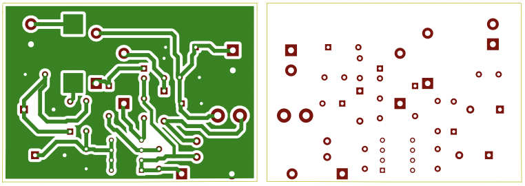
Figure 7. We have made the PCB of this circuit using KICAD.
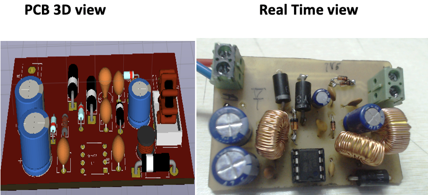
Figure 8. PCB files.
Video
You may also like:


Filed Under: Tutorials
Log in to leave a comment:
Lost your password?
Don't have an account? Register here