The previous tutorials laid the foundation for logic synthesis and design of digital circuits. The digital circuits in general always have application as computing devices either as processor, controller or application specific ICs. As a computing device, the digital circuitry of a processor, controller or ASIC must be essentially able to perform arithmetic operations. The implementation of arithmetic operations by digital circuitry is further used to build up complex computing logics and mathematical functions.
In a processor/controller/ASIC, the arithmetic operations on integer binary numbers are performed by Arithmetic Logic Unit (ALU) while arithmetic operations on floating point numbers are performed by Floating Point Unit (FPU). A Floating Point Unit itself is built from multiple ALUs. Within a Central Processing Unit (CPU) or Graphics Processing Unit (GPU) of a computer/computing device, there are many ALU and/or FPU (where FPU themselves are built from multiple ALU).
The digital circuits can be either of the two types – 1) Combinational Logic Circuits or 2) Sequential Logic Circuits. In a combinational circuit, the output of the circuit depends only on the input values at that time. In sequential circuits, the output depends not only on the present input but also past output values. The ALU are built by combinational circuits. The ALU is typically designed to perform the following operations:
1) Arithmetic Operations – Generally, the arithmetic operations supported by the ALU are addition, addition with carry, subtraction, subtraction with borrow, two’s complement, increment, decrement and pass through.
2) Bitwise Logical Operations – The logical operations supported by the ALU are AND, OR, Exclusive-OR and One’s Complement.
3) Bit Shift Operations – The bit shift operations implemented in an ALU include arithmetic shift, logical shift, rotate and rotate through carry.
So, ALU can perform arithmetic operations like addition and subtraction, and so multiplication and division on integer binary numbers. A binary number may be available to the ALU of a digital processor either as parallel 8-bit, 16-bit, 32-bit or 64-bit input depending upon if it is 8-bit, 16-bit, 32-bit or 64-bit processor. The basic building blocks of the ALU are adders. The adder circuits are built by logic gates and flip-flops. The semiconductor adder circuits can perform addition in a time less than 1 microseconds.
Let us learn about various combinational circuits – half-adder, full-adder, half-subtractor, full-subtractor, N-bit parallel adder, N-bit parallel subtractor etc that are generally part of an ALU.
Half Adder –
The half adder is a simple combinational circuit which performs the arithmetic addition of two binary digits or addition of two bits. It has two inputs and two outputs. The two inputs are the two 1-bit numbers A and B while the two outputs are the sum (S) of A and B and the carry (C). The truth table for a half adder is as follow –
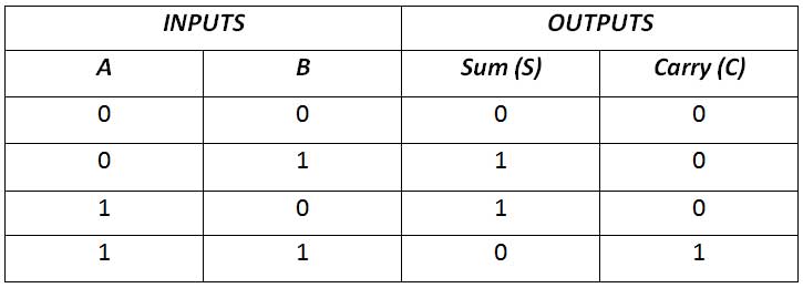
Fig. 1: Truth Table of Half Adder
From the above truth table, it must be clear that the sum is 1 if either of the two inputs is 1 else if both inputs are 1 or 0, the sum is 0. This can be implemented by connecting the inputs to an exclusive OR gate. The carry is 1 only if both inputs are 1 else it is 0. This can be implemented by connecting the inputs to AND gate. So, the half adder has the following circuit –
Fig. 2: Symbol and Logic Gate Diagram of Half Adder
Full Adder –
A half adder has only two inputs and there is no provision to add a carry coming from the lower order bits when multiple bit addition is performed. For this purpose full adder is designed. A full adder is designed to perform the arithmetic sum of three input bits and produces a sum output and a carry. The truth table for a full adder is as follow –
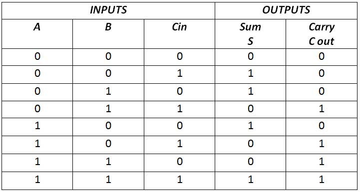
Fig. 3: Truth Table of Full Adder
From the truth table, it must be clear that the full adder has three inputs and two outputs. The two input variables are denoted by A and B, which represents the two significant bits to be added. The third input Cin represents the carry from the previous low significant position. The outputs aresum (S) and Carry (C). From the truth table, it can be seen that Sum is 1 if either input is 1 or all inputs are 1. This can be implemented by exclusive-OR of all the inputs. The carry is 1 when either two inputs are 1 or all inputs are 1. This can be implemented as sum of product expression of all the inputs. So, the full adder has the following circuit –

Fig. 4: Symbol and Logic Gate Diagram of Full Adder
It can be noted that full adder is formed by two half adder circuits and an OR gate.
Half Subtractor –
The half subtractor is a simple combinational circuit designed to perform subtraction of two bits. It has two inputs, X and Y and two outputs Difference (D) and Borrow out (Bout). The truth table for a half subtractor is as follow –
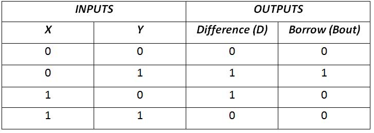
Fig. 5: Truth Table of Half Subtractor
From the truth table, it can be seen that the difference D is 1 if either input is 1 else if both inputs are 1 or 0, the D is 0. This can be implemented by connecting the inputs to an exclusive OR gate. The Borrow Out (Bout) is 1 only if Y is 1 but not X. The borrow output Bout is 1 whenever X is lesser than Y, then the subtraction is done by borrowing 1 from the next higher order bit. This can be implemented by AND operation between Y and NOT of X. So, the half subtractor has the following circuit –

Fig. 6: Symbol and Logic Gate Diagram of Half Subtractor
Full Subtractor –
A full subtractor is designed to perform subtraction involving three bits, namely minuend bit, subtrahend bit and borrow from previous stage. In full subtractor, it has three inputs X, Y and Bin, and two outputs Difference (D) and Borrow (Bout). It has the following truth table –
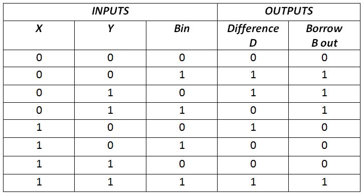
Fig. 7: Truth Table of Full Subtractor
From the truth table, it can be seen that Difference is 1 if either input is 1 or all inputs are 1. This can be implemented by exclusive-OR of all the inputs. The Borrow Out is 1 if either two inputsis 1 or all inputs are 1. This can be implemented as OR operation between two half subtractor. So, the full subtractor has the following circuit diagram –

Fig. 8: Symbol and Logic Gate Diagram of Full Subtractor
N-Bit Parallel Adder –
The Full Adder is capable of adding only two single digit binary number along with a carry input. Practically, there is need to add binary numbers which are much longer than just one bit. To add two n-bit binary numbers there need to use the n-bit parallel adder. It uses a number of full adders in cascade. The carry output of the previous full adder is connected to carry input of the next full adder.
Like a 4-bit parallel adder, can be constructed by cascading four full-adder circuits. In the circuit A0 and B0 represent the LSB of the four bit words A and B where Full Adder-0 is the lowest stage. Hence its Cin has been permanently made 0. The rest of the connections are exactly same as those of n-bit parallel adder. The four bit parallel adder is a very common logic circuit. A 4-bit parallel adder can be shown by the following block diagram –

Fig. 9: Logic Gate Diagram of 4-Bit Parallel Adder
N-Bit Parallel Subtractor –
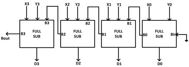
The subtraction can be carried out by taking the 1’s or 2’s complement of the number to be subtracted. For example, the subtraction (A-B) can be performed by adding either 1’s or 2’s complement of B to A. So, a binary adder can be used to perform the binary subtraction. Just as a parallel binary adder can be implemented by cascading several full adders, a parallel binary subtractor can also be implemented by cascading several full subtractors.
Like a 4 – bit binary parallel subtractor that subtracts a 4 – bit number Y3 Y2 Y1 Y0 from another 4 – bit number X3 X2 X1 X0 will have 4 difference outputs and borrow output (Bout). The Bin of the LSB full subtractor is connected to 0 and Bout of previous full subtractor is connected to Bin of next full subtractor. A 4-bit parallel subtractor can be shown by the following block diagram –
Fig. 10: Logic Gate Diagram of 4-Bit Parallel Subtractor
In the next tutorial, learn about gate level minimization and logic gate implementation of the arithmetic circuits discussed above.
Filed Under: Digital Electronics, Tutorials



Questions related to this article?
👉Ask and discuss on EDAboard.com and Electro-Tech-Online.com forums.
Tell Us What You Think!!
You must be logged in to post a comment.