In the previous tutorial, encoder and decoder circuits were built using SN-7400 series logic gate ICs. The multiplexer and demultiplexer are also combinational circuits similar to encoder and decoder. A multiplexer is a circuit that accepts many inputs and channelize digital data to only one output. The combinational circuit of a multiplexer is similar to encoder with only difference that the multiplexer has select inputs that determine from which input the data should be channelized to the output. Like encoder, a multiplexer circuit can be built using AND, NOT and OR gates.
A demultiplexer functions exactly opposite of a multiplexer, i.e. a demultiplexer accepts only one input and channelize data to many outputs. The combinational circuit of demultiplexer is similar to decoder except that demultiplexer has select inputs that determine to which output line input binary data must be channelized. Like decoder, demultiplexer circuit can be built using AND gates and NOT gates.
The multiplexers are used in telephony, communication systems and computer memories. They are also used as parallel to serial data converters. The demultiplexers are used in communication systems, computers chips for connecting ALU with registers and in serial to parallel converters. In communication systems, since the data communication is always bidirectional, both multiplexer and demultiplexer are used together. In such systems, the multiplexer and demultiplexer used are designed to be compatible to each other.
In this tutorial, a 4-input multiplexer and a 4-output demultiplexer are designed. The 4-input multiplexer has 4 input lines, 2 select inputs and one data input. The 4-output demultiplexer has one data input, 2 select inputs and 4 outputs.
Components Required –
![]()
Fig. 1: List of components used for making SN-7400 Series IC based Multiplexer and Demultiplexer
Circuit Diagram –
The multiplexer has the following circuit diagram –
![]()
Fig. 2: Circuit Diagram of 4:1 Multiplexer
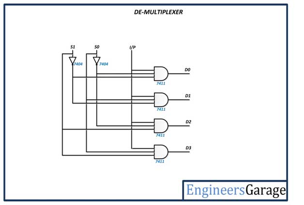
The demultiplexer has the following circuit diagram –

Fig. 3: Circuit Diagram of 1:4 Demultiplexer
Circuit Connections –
The multiplexer and demultiplexer are also combinational circuits. Their output depends only on the current value of inputs. Each circuit has a unique truth table from which the respective boolean expression for each output can be derived. The minimized boolean expression is then converted into logic gate diagram which is built on a breadboard using 7400 series ICs.
The following logic gate ICs are used in the construction of the circuits –
7411 IC – The 7411 IC is triple 3-input AND gate IC. The IC has the following pin configuration –
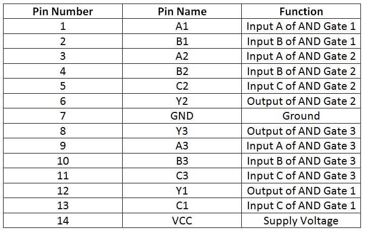
Fig. 4: Table listing pin configuration of 7411 IC
The IC has the following pin diagram –
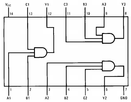
Fig. 5: Pin Diagram of 7411 IC
The IC requires a supply voltage of 5V which can be tolerated up to 5.25V. The voltage at the inputs of AND gates must be 2V for high logic and 0V for low logic. The output of the AND gates has a voltage of 3.4 V for high logic and up to 0.8 V for low logic. The IC operates on positive logic system. The propagation delay while transiting from LOW to HIGH level at the output ranges between 4 to 18 ns while propagation delay while transiting from HIGH to LOW level at the output ranges between 3 to 18 ns.
7432 IC – The 7432 IC has quad 2-input OR gates. The IC has the following pin configuration –
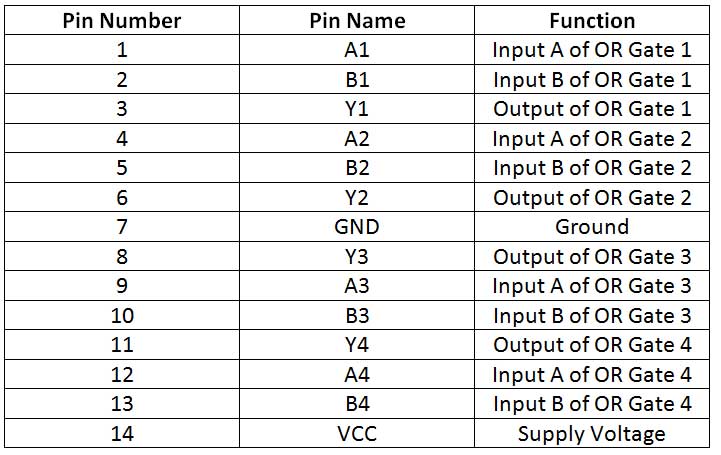
Fig. 6: Table listing pin configuration of 7432 IC
The IC has the following Pin Diagram –
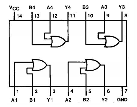
Fig. 7: Pin Diagram of 7432 IC
The IC requires a supply voltage of 5V which can be tolerated up to 7V. The voltage at the inputs of OR gates must be 2V for high logic and 0V for low logic. The output of the OR gates has a voltage of 3.4 V for high logic and 0.35 V for low logic. The IC operates on positive logic system. The propagation delay while transiting from LOW to HIGH level at the output comes 3 to 15 ns while propagation delay while transiting from HIGH to LOW level at the output also comes 3 to 15 ns.
7404 IC – The 7404 IC has six inverting gates. The IC has the following pin configuration –
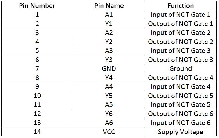
Fig. 8: Table listing pin configuration of 7404 IC
The IC has the following Pin Diagram –
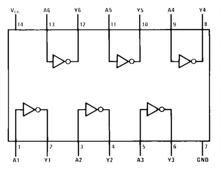
Fig. 9: Pin Diagram of 7404 IC
The IC requires a supply voltage of 5V which can be tolerated up to 7V. The voltage at the inputs of NOT gates must be 2V for high logic and 0.8 V for low logic. The output of the NOT gates have a voltage of 3.4 V for high logic and 0.2 V for low logic. The IC operates on positive logic system. The propagation delay while transiting from LOW to HIGH level at the output is 22 ns while propagation delay while transiting from HIGH to LOW level at the output is 15 ns.
It must be noted that the selected ICs have compatible input, output and supply voltage levels as they are taken from a common family (74XX series) of digital ICs.
How the circuit works –
For constructing the multiplexer and demultiplexer circuit, first of all, their truth table must be known. From the truth table, the boolean expressions for each output line can be derived. The boolean expression relates the output variables with the input variables by respective boolean equation. The derived boolean equations can be realized by interconnecting logic gates accordingly. The multiplexer and demultiplexer circuits are constructed as follow –
Multiplexer – Multiplexer means transmitting a large number of information units over a smaller number of channels or lines. A digital multiplexer is a combinational circuit that selects binary information from one of many input lines and directs it to a single output line. The selection of a particular input line is controlled by a set of selection lines. Normally there are 2n input lines and n number of selection lines whose bit combination determines which input must be selected. A 4-input multiplexer is designed here which has 4 inputs, 2 select inputs and one output line. It has the following truth table –

Fig. 10: Truth Table of 4:1 Multiplexer
The multiplexer has the following function table –

Fig. 11: Function Table of 4:1 Multiplexer
From the truth table, the multiplexer can be constructed using AND gates, NOT gates and OR gates. Since there are two select pins and data from each input is routed through one AND gate, 3-input AND gates are required for the circuit. Here, for constructing the multiplexer circuit, 7404 IC for NOT gate, 7411 IC for AND gate and 7432 IC for OR gate are used.

Fig. 12: Prototype of 4:1 Multiplexer
Multiplexers are used in various applications where data from many input channels need to be transmitted on a single line. The multiplexers are used in the following electronic applications –
Communication systems – Communication system is a set of system that enables communication between two points or locations like transmission system, relay and tributary station, and communication networks. The efficiency of communication system can be increased considerably using multiplexer. Multiplexer allows the process of transmitting different type of data such as audio, video at the same time using a single transmission line.
Telephone network – In telephone networks, multiple audio signals are integrated on a single line for transmission with the help of multiplexers. In this way, multiple audio signals can be isolated and eventually, the desired audio signals reach the intended recipient.
Computer memories – Multiplexers are used to implement huge amount of memory into the computer systems by reducing the number of copper lines required to connect the memory to other parts of the computer circuit at the same time.
Transmission from the computer system of a satellite – Multiplexer can be used for the transmission of data signals from the computer system of a satellite or spacecraft to the ground system using the GPS (Global Positioning System) satellites.
Demultiplexer – The function of a Demultiplexer is opposite to multiplexer function. It takes information from one line and distributes it to a given number of output lines. For this reason, the demultiplexer is also known as a data distributor. A decoder can also be used as demultiplexer.
In the 1: 4 demultiplexer circuit, the data input line goes to all of the AND gates. The data select lines enable only one gate at a time and the data on the data input line passes through the selected gate to the associated data output line. The 1:4 demultiplexer has the following truth table –

Fig. 13: Truth Table of 1:4 Demultiplexer
The demultiplexer has the following function table –

Fig. 14: Function Table of 1:4 Demultiplexer
From the truth table, the demultiplexer can be constructed using AND gates and NOT gates. Since there are two select pins and one data input, 3-input AND gates are required for the circuit. Here, for constructing the demultiplexer circuit, 7404 IC for NOT gate and 7411 IC for AND gates are used.

Fig. 15: Prototype of 1:4 Demultiplexer
The demultiplexer is used to connect a single source to multiple destinations. The main application of demultiplexer is in communication systems where multiplexer are also used at the transmission end. Most of the communication systems are bidirectional i.e. they send and receive data both ways (transmitting and receiving signals). Hence, for most of the applications, the multiplexer and demultiplexer work in sync. Demultiplexers are also used for reconstruction of parallel data and ALU circuits. The demultiplexers have the following applications –
Communication Systems – Communication systems use multiplexer to carry multiple data like audio, video and other form of data using a single line for transmission. This process makes the transmission easier. The demultiplexer receives the output signals of the multiplexer and converts them back to the original form of the data at the receiving end. The multiplexer and demultiplexer work together to carry out the process of transmission and reception of data in a communication system.
ALU (Arithmetic Logic Unit) – In an ALU circuit, the output of ALU can be stored in multiple registers or storage units with the help of demultiplexer. The output of ALU is fed as the data input to the demultiplexer. Each output of demultiplexer is connected to multiple registers where data can be stored in them.
Serial to Parallel Converter – A serial to parallel converter is used for reconstructing parallel data from incoming serial data stream. In this technique, serial data from the incoming serial data stream is given as data input to the demultiplexer at the regular intervals. A counter is attaching to the control input of the demultiplexer. This counter directs the data signal to the output of the demultiplexer where these data signals are stored. When all data signals have been stored, the output of the demultiplexer can be retrieved and read out in parallel.
Testing the circuits –
The circuits designed above can be tested by giving supply voltage to the ICs by a battery via 7805 voltage regulator. The same voltage can be dropped to 2V level using a variable resistor for HIGH logic while providing LOW logic through ground. The output signals can be checked by connecting LEDs at the output pins of each combinational circuit. The circuits can be checked by verifying truth tables for each circuit.
In the next tutorial, learn about sequential logic circuits.
Circuit Diagrams

Filed Under: Digital Electronics, Tutorials
Log in to leave a comment:
Lost your password?
Don't have an account? Register here