Frequency modulation (FM) is a technique in which the frequency of a transmitted waveform is varied according to the variations in the message wave. The FM is a very popular technique since they are widely used by the FM radio stations. The main reason behind using the FM modulations by the radio stations is the quality of the signal that can be recreated in the FM receiver. The signal to noise ratio is comparatively very high at the output of FM demodulator circuits. However the FM modulator and demodulator circuits are complex compared to other modulation and demodulation techniques.
The FM demodulator is done with the help of a circuit called Phase Locked Loop (PLL). A PLL should have basic functional blocks like Voltage Controlled Oscillator (VCO), Phase comparator, Low Pass Filter (LPF) and Source follower. In the demodulator circuit the VCO generates a frequency which matches the original carrier frequency and compares the phase of that with received FM wave using the Phase comparator. The output of the Phase comparator is filtered out using the LPF and is current amplified using a Source follower. The output of the source follower matches the original message signal.
To implement all the above mentioned circuitry is a difficult task, but there are ICs available which has all these circuit blocks embedded in it. In this article the FM demodulation circuit is made with the help of a PLL IC called HEF4046.
SUMMARY:
The HEF4046B is a 16 pin DIP IC which works on 3 V to 15 V DC. It has built-in phase-locked loop (PLL) circuit that consists of a linear Voltage Controlled Oscillator (VCO) and two different Phase comparators. The Low Pass Filter (LPF) has to be connected externally to the IC. This IC can recreate the FM signals with good quality using only a few external components. The functional diagram of the IC is given below:
The C1 is the capacitor and R1 and R2 are the resistors on which the VCO depends on its output frequency. The value of the C1, R1 and R2 should be selected in such a way that the VCO produces pulses which matches the original un-modulated carrier frequency of the FM wave. The resistors R3 and C2 form the external Low Pass Filter (LPF), the cut of frequency of which depends on the value of R3 and C2. The value of the R3 and C2 should be selected in such a way that the RC constant should match the range of the frequencies at which the message signals can be expected.
In this project the FM modulation of a pure sine wave is done with the help of a 555 IC wired as a VCO. The pure sine wave is generated using a Wien Bridge Oscillator (WBO) which is then clamped to the positive voltage side using a positive clamper circuit. This signal is then applied to the 555 VCO circuit to generate the corresponding FM wave.
The block diagram of the entire set up for FM generation is shown in the following diagram:
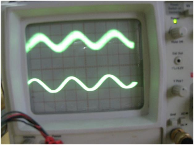
Fig. 1: Block Diagram Of FM generation circuit
The WBO circuit is designed to generate pure sine wave of 1 KHz with peak-to-peak amplitude around the supply voltage of 5V. The WBO circuit and the image of the waveform generated is shown in the following figure:

Fig. 2: Circuit Diagram Of Wien Bridge Oscillator (WBO)

Fig. 3: Sine Wave from Wien Bridge Oscillator (WBO) On CRO Screen
Clamper and Amplifier
A positive clamper circuit follows the sine wave generator and is made using a single capacitor and diode. The clamper circuit and the clamped sinusoidal waveform are shown in the following figure:

Fig. 4: Circuit Diagram of Positive Clamper

Fig. 5: Sinusoidal Waveform from Clamped circuit On CRO Screen
The clamping circuit is followed by a potential divider and current amplifier. The significance of the potential divider here is that by adjusting the entire amplitude of the signal input to the 555 VCO, the range at which the frequency varies in the FM produced can be adjusted. The clamper circuit with potential divider and current amplifier is shown below:

Fig. 6: Circuit Diagram Of Clamper With Potential Divider And Current Amplifier
A 555 timer IC is wired as a normal astable mutivibrator with constant on-off time period. The only difference in this circuit is that the pin number 5 is not connected to the positive via a capacitor, but it is used to receive the modulating signal. The voltage at the pin number 5 of the 555 timer IC controls the frequency generated by the astable circuit and since the voltage applied here at the pin 5 is a sine wave of 1 KHz the output pulse frequency varies according to the sinusoidal variations in the amplitude. The circuit diagram of the 555 modulator is given in the following diagram:

Fig. 7: Circuit Diagram Of 555 Modulator
The un-modulated frequency of the pulses generated by the above circuit can be calculated using the following equation:
F = 1.44 / ( ( R1 + R2 ) * C1 )
Applying the value of R1 = R2 = 1K and C1 = 0.1uF, the frequency can be calculated as 7.2 KHz.
Hence the frequency of the pure sine wave of 1 KHz and it is now modulated with a varying frequency pulses which have a center frequency around 7 KHz.
The 555 modulator circuit is connected with the previous positive clamper circuit through a 1uF polarized capacitor. The entire circuit diagram and the image of the circuit wired in the bread board is shown in the following figure:

Fig. 8: Circuit Diagram of FM Generation

Fig. 9: Circuit of FM Generation On Breadboard
FM Demodulation Circuit
As the amplitude variations occurs in the sine wave the frequency generated by the 555 changes and hence a frequency modulated wave is obtained at the output of the 555 IC. As the amplitude increase the frequency decreases and vice versa. For large amplitude signals the frequency variation will be large and for small amplitude signals the frequency variations will be small. The amplitude of the sine wave signal applied to the 555 modulator can be varied by varying the 1M ohm potentiometer. The following is the image captured from the dual channel CRO where the FM wave is displayed in above and the original sine wave which is used to modulate them is displayed below.

Fig. 10: Waveform Generation Of FM With Original Sine Wave On CRO
Since the original pulse frequency is around 7 KHz the HEF4046 IC based demodulator can be designed to receives pulses in the frequency range of 2 to 12 KHz. Here the minimum frequency (Fmin) is assumed to be 5 KHz and the maximum frequency (Fmax) is assumed to be 10 KHz.
The functional diagram of the IC is added here again for calculate the values of the components:
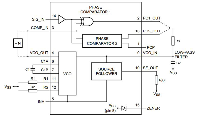
Fig. 11: Functional Diagram Of IC
The frequency offset as a function of C1 with minimum frequency (Fmin) plot is available in the datasheet of the IC and from that the value of R2 and C1 is selected.

Fig. 12: Supply Voltage Graph Of 5V
From the graph for a supply voltage of 5V, Fmin = 5KHz occurs for R2 = 10K and C1 = 0.01uF.
Another graph is plotted based on the value of the R2 / R1 and Fmax / Fmin from which the value of R1 can be find out.

Fig. 13: Graph for R2 / R1 and Fmax / Fmin
Here the Fmax / Fmin = 5, and for a 5V supply it occurs for an R2 / R1 = 10. Since the value of R2 is already found out as 10 K, R1 can be calculated as 1 K.
The R3 and C2 forms the LPF and its time constant i.e R * C should be in the range of inverse of the message frequency i.e 1 / Fmsg.
Assume R = 1K, since frequency of sine wave message Fmsg = 1 KHz
1000 * C = 1 / 1000
From which C = 1uF can be calculated.
With that all the components values has been designed and the complete circuit design for the FM demodulation is shown in the following: An additional input coupling capacitor 0.1uF is used to couple the signals to the input of the IC and a 1K resistor is used at the output of the IC as a load resistor.
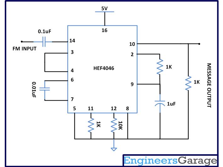
Fig. 14: Circuit Diagram of FM Demodulation
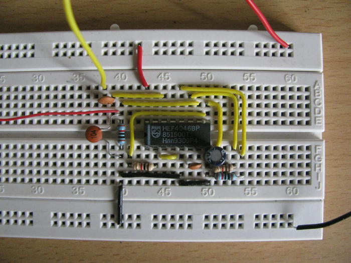
Fig. 15: FM Demodulation Circuit On Breadboard
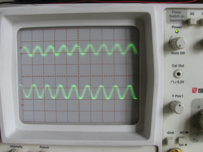
Fig. 16: Waveform Of Original Message And Demodulation of FM On CRO
The original message waveform and the demodulated waveform are plotted in a dual channel CRO as shown below. It can be observed that the two waveforms are similar and the noise effect is very low. An additional 0.1uF can be connected across the output load resistor to avoid noise even more.
The images of the FM modulator circuits and demodulator circuits wired in the breadboard are shown below:
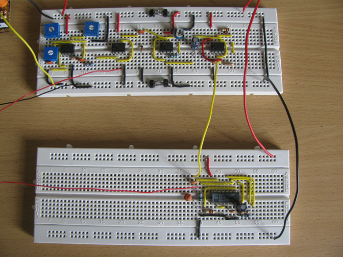
Fig. 17: FM Modulator Circuits And Demodulator Circuit On Breadboard
Filed Under: Circuit Design


Questions related to this article?
👉Ask and discuss on Electro-Tech-Online.com and EDAboard.com forums.
Tell Us What You Think!!
You must be logged in to post a comment.