In the previous tutorial, square wave inverter was designed. Square wave inverter was simple to design but had certain drawbacks. The AC appliances are actually designed to operate on sine wave and square wave though being AC signal does not match to an ideal sine wave. Due to this, when an appliance is powered by a square wave inverter, it may have noise or humming sound during its operation. So, designing of a modified sine wave inverter will be discussed in this tutorial.
The modified sine wave inverter is just another inverter design which has an output waveform which approximates to an ideal sine wave. Being an inverter it converts DC into AC. So, the power is drawn by the modified sine wave inverter from a battery and it converts the DC power to AC power.
In fact, the output of a modified sine wave inverter is a combination of two square waves having a phase difference of 90 degrees superimposed over each other. As a result, contrary to a square wave which has only two voltage levels (peak to peak voltages), the resultant wave has three voltage levels – positive peak, zero level and negative peak. The output waveform of such inverter can be termed as quasi sine wave. The modified sine wave take a pause (set at zero volts) before changing the polarity (as shown in the image below).
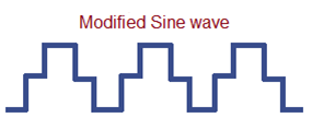
Fig. 1: Signal Diagram of Modified Sine Wave
The output of such inverter can be used to drive low sensitive AC devices. It is important to understand that the AC appliances are meant to be run on AC supply with certain specifications. Every country maintains its own standards for main supplies. But most of the countries have power supply having frequency from 50 Hz to 60 Hz. The supply usually has symmetric waveform and the voltage level ranges from 120 V to 220 or 230 V. This is the general standard in most of the countries. According to the Indian standards for driving AC loads, the AC supply must be of the frequency 50Hz with the symmetrical AC waveform and the voltage of the AC should be in between 220 V to 240 V. The European Union has similar standards. In United States and Canada, the mains voltage should be 120 V with 5 percent tolerance at 60 Hz frequency.
As according to the Indian standards, the AC appliances are meant to work efficiently at a frequency of 50Hz and voltage between 220V to 240V AC, in this tutorial, a sine wave generator having 50 Hz frequency will be designed. The acceptable deviation in the frequency can be +/- 0.5 Hz.
A symmetrical waveform has the same time period for both the halves of the cycle whereas in an asymmetric waveform, the time period of positive and negative cycle are different. If an unsymmetric AC wave is applied to an AC appliance which converts the electrical energy into mechanical energy like motor then it will experience jerks during its rotary motion. So it is necessary that the AC waveform should be symmetric in nature.
The modified sine wave inverter designed here will use Arduino and a gate driver circuit. The basic concept of such inverter will be discussed in this tutorial and then the designing of the actual inverter circuit will be discussed from the next tutorial. Designing a modified sine wave inverter having an output frequency of 50 Hz and peak voltage 220V will be the aim of this project.
Block Diagram of Modified Sine Wave Inverter –
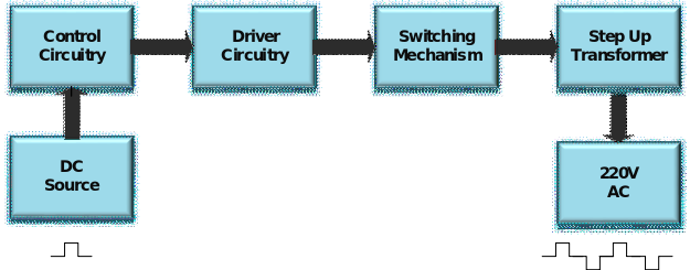
Fig. 2: Block Diagram of Modified Sine Wave Inverter
Construction of Modified Sine Wave Inverter –
The design of a modified sine wave inverter can be divided into following building blocks –
DC source – A 12V battery will be used to draw power by the inverter. The power drawn from the battery will only be converted to AC power.
Control Circuitry – This is an intelligent circuitry which will be used to drive a transistor circuit for the generation of modified sine wave. This circuit can itself be built using transistors or can be built using a controller board. It is quite easier to built such control circuit with the help of a microcontroller as it avoids designing a complex transistor circuit for the same purpose. In the designing of this inverter, Arduino UNO will be used for control circuit.
Driver Circuitry – The generation of modified sine wave involves driving a gate driver circuit from the control circuitry. A modified sine wave having lower peak to peak voltage is first generated by the gate driver circuit which is then stepped up to 220 V level. The IR2110 IC is used as gate driver for the MOSFET circuit involved in generation of the modified sine wave.
Switching Mechanism – An inverter supplies power to a load when main supply is cut off. So, the inverter requires a switching mechanism between the gate driver circuit to generate a perfect AC signal and resume supply when the main power is cut.
Step Up transformer – The output from the MOSFET circuit is a modified sine wave having a lower peak to peak voltage. This AC wave needs to be stepped up to 220 V level using a step up transformer.
How a Modified Sine Wave Inverter works –
There are various methods for generation of modified sine wave like by using transistors with other basic components or by using a microcontroller board. The transistor method increases the complexity as it requires designing a complex circuit of transistors and basic electronic components. The use of microcontroller for generation of quasi sine wave is an easier alternative as any microcontroller is readily capable of controlling any TTL circuit by generating appropriate digital output from its GPIO pins. In the transistor method, such logic will have to be generated by designing an elaborate transistor circuit which is neither easy nor error free. So, the controller method will be used to generate the modified sine wave.
The basic elements of such inverter are the Arduino board (or any other microcontroller board) and a MOSFET circuit.
(as shown in figure below).
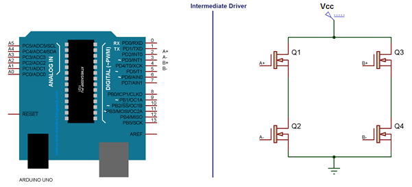
Fig. 3: Image showing components used for making Modified Sine Wave Inverter
Here the Arduino is not directly connected to the gate of FETs, as it needs some intermediate gate driver circuit which switches the FETs. But the controller indirectly controls the gate of all FETs with the help of an intermediate gate driver IC. The basic operation of this modified sine wave inverter is all about how the controller operates the four FETs to generate an output waveform which has three voltage levels where all FETs work as logical switches. The operation of intermediate gate driver circuit will be discussed in the next tutorial.
For generating a modified sine wave, the Arduino board is used as the controller board. The Arduino is the most popular protyping board which is easily available and easy to use. The Arduino UNO has the Atmega 328 as the sitting MCU. As mentioned before, modified sine wave has three levels (zero, positive and negative). So for generating a modified sine wave the Arduino must be programmed to generate appropriate digital logic from its GPIO pins connected indirectly with the gates of the FETs. The digital output from the controller ultimately switches the FETs on and off genearting a modified sine wave at the output.
The Arduino code for generating such digital output looks like as shown in the figure below –
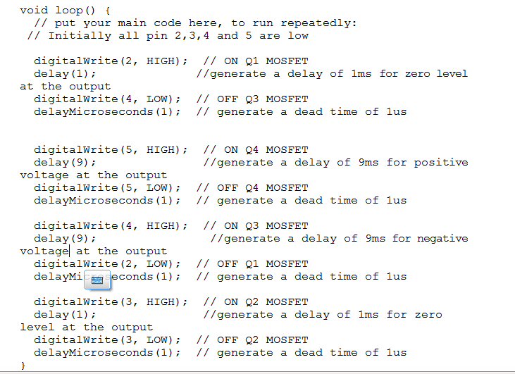
Fig. 4: Screenshot of Arduino Code used for Modified Sine Wave Inverter
The above code is written with the understanding that the Arduino pins are interfaced with the MOSFET gate terminals via an intermediate gate driver IC in the following fashion (as shown in figure above) –
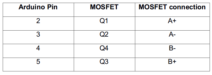
Fig. 5: Table listing circuit connections between Arduino and MOSFET
The digital output generated from the Arduino drives the MOSFETs according to the following truth table –

Fig. 6: Truth Table for Modified Sine Wave Inverter
So, the MOSFET are used in the circuit for switching purpose as they are faster than BJT. The base of BJT transistors store minority carriers during saturation state, because of which these minority carriers take some time to flush out when BJT is in OFF state. This increases the response time of BJT transistors. While FET transistors do not have any such problem.
Initially, all the MOSFETs are OFF. When the first statement in the code is executed followed by the delay statement of 1 ms then the transistors Q1 and Q3 turns ON and transistors Q2 and Q4 still remain in the OFF state. This makes both the load terminals ‘e’ and ‘f’ at the same potential (as shown in the image below). So zero volts is output across the load for around 1 ms. A modified sine wave without a zero level is equivalent to the square wave. The RMS and peak to peak voltage of the modified sine wave are equal to the pure sine wave due to the zero volt level of the modified sine wave. Therefore, the zero level is must for generating a modified sine wave which resembles to the pure sine wave. The zero level should have minimum time period so that maximum duty cycle can be achieved.
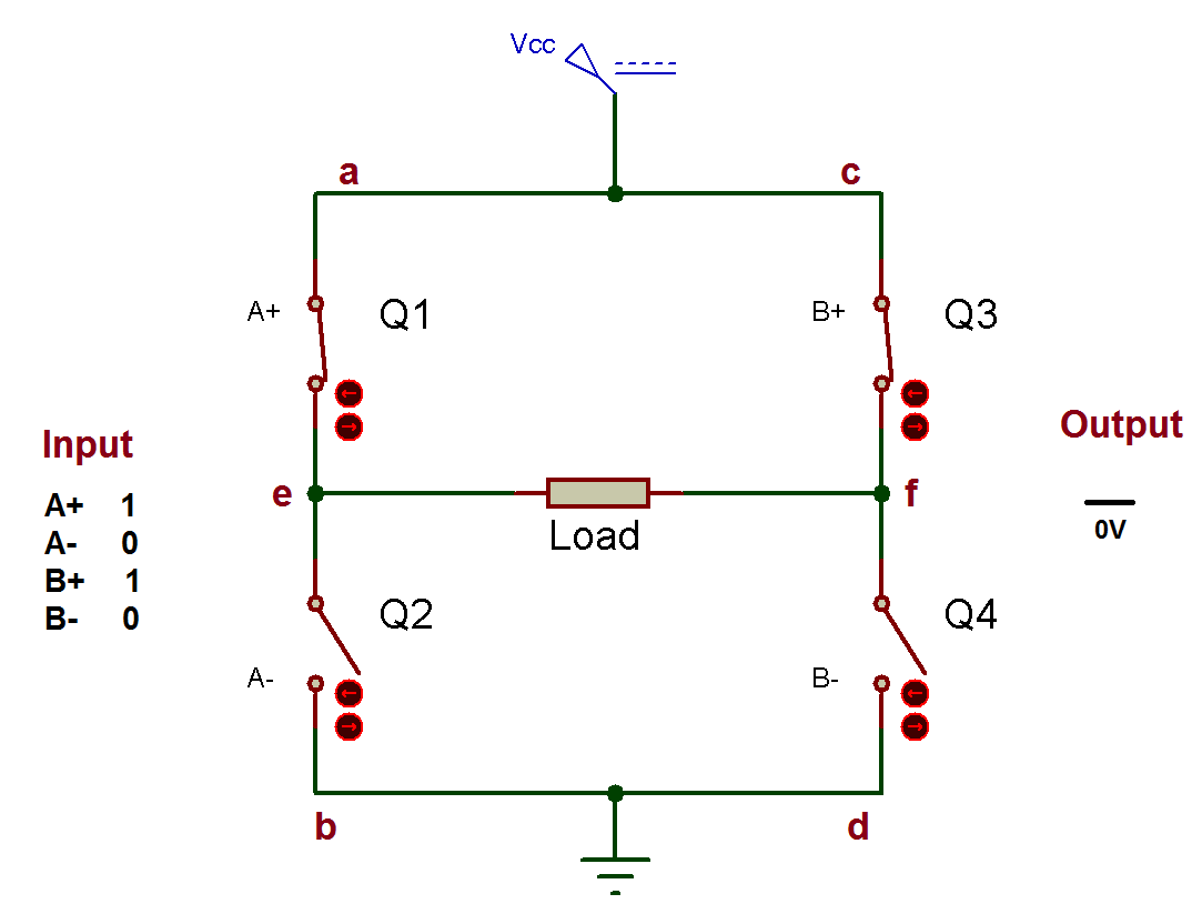
Fig. 7: Circuit Diagram showing Working of H-Bridge MOSFET circuit in Modified Sine Wave Inverter at Zero Volt level
Now the transistor Q3 is turned off following a delay of 1 us. This 1 us delay is called dead time. The dead time is necessary so that transistors Q1 and Q2 or Q3 and Q4 should not turn ON simultaneously. The simultaneous switching of the transistors can short the supply. Then, the transistor Q4 is turned ON for about 9 ms. This turns ON the transistor Q1 and Q4 for 9 ms while the transistors Q3 and Q2 are turned OFF. Therefore the current starts following from point ‘a’ to point ‘d’ through the load (as shown in the figure below). This makes the left terminal of the load at high potential than its right terminal and a positive voltage (+Vcc) is output across the load for around 9 ms.
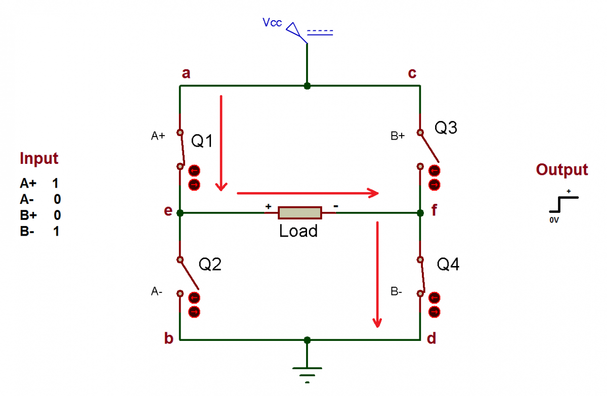
Fig. 8: Circuit Diagram showing Working of H-Bridge MOSFET circuit in Modified Sine Wave Inverter at Positive Voltage level
Now again the transistor Q4 is turned OFF with a dead time of 1 us and the transistor Q3 is turned ON for 1 ms. This generates the 0 V level at the output and the output waveform changes from positive peak (+Vcc) to zero volt level (0 V) (as shown in image below).
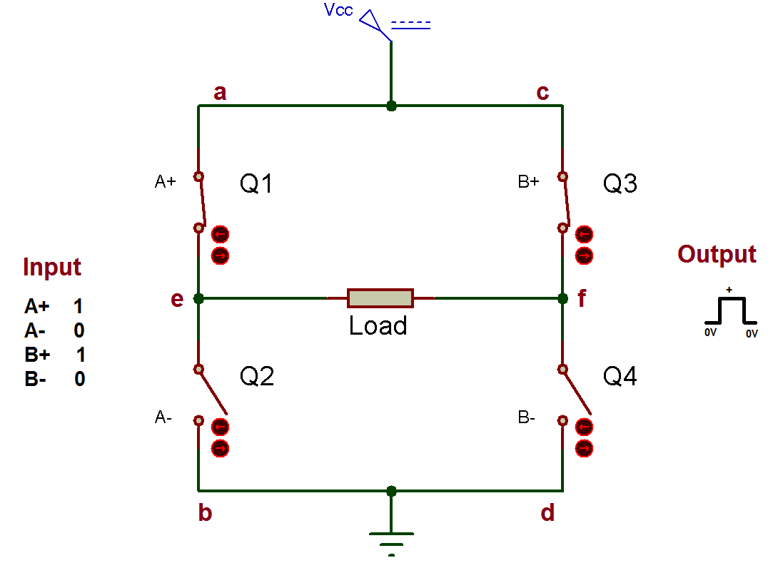
Fig. 9: Circuit Diagram showing Working of H-Bridge MOSFET circuit in Modified Sine Wave Inverter at Change of Polarity
Now the transistor Q1 is turned OFF with a dead time of 1 us and the transistor Q2 is turned ON for 9 ms. Now the direction of flow of current is from point ‘c’ to point ‘b’. This makes the right terminal of the load at high potential than its left terminal. So, a negative voltage (-VCC) is output across the load and this changes the output waveform from 0 V to negative volt for around 9 ms.
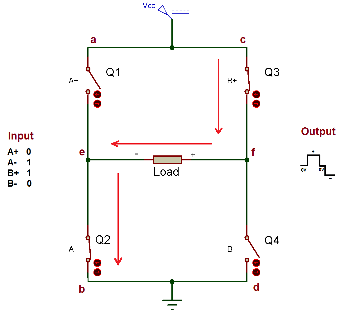
Fig. 10: Circuit Diagram showing Working of H-Bridge MOSFET circuit in Modified Sine Wave Inverter at Negative Voltage level
So, the transistors are switched on and off as shown in the truth table above. The code statements are written in the main loop of the Arduino sketch so, it repeats itself infinitely and a 12V modified sine wave with 50 Hz frequency is obtained at the output. It should be noted that this circuit cannot be implemented without a gate driver circuitry. The gate driver circuit is discussed in the next tutorial.
It is important that to avoid any shoot through current or short circuit current, dead time must be generated the microcontroller code. The short-circuit current occurs when both the MOSFET (transistors Q1 and Q2) or (transistors Q3 and Q4) turn ON simultaneously. This eventually causes the loading and can damage the inverter. Therefore dead time should be provided between two signals, both at the rise and falling edge of the MOSFET. The Dead time should not be increased too much as it can decrease the duty cycle of the signal. From hardware aspect, it must be made sure that the Arduino back surface does not touch any metal surface since it can flow small current beneath it and may damage the controller board. The input voltage of the Arduino should not exceed 12 V level as that is the maximum supply voltage allowed according to its technical specifications. Applying a voltage above this may damage the board permanently. The Arduino board must be powered only by a regulated DC source as the controller is designed to operate on DC power. While loading the executable code to the controller board, it must be made sure that the board used in the circuit is correctly selected in the Arduino IDE. The right board can be selected by navigating to Tools->Boards->select option from the main menu of the IDE. While uploading the code, the USB connector from the PC should be removed in between otherwise, the executable code will not load properly on the board.
In the next tutorial, the designing of gate driver circuit for the modified sine wave inverter will be discussed.
Project Source Code
###


//Program to

//* Code for generating Modified Sine Wave*//

void setup() {

  // Setting  all four MOSFET as output

pinMode(2, OUTPUT); //  A+ gate of Q1 MOSFET

pinMode(3, OUTPUT); // A- gate of Q2 MOSFET


pinMode(4, OUTPUT); // B+ gate of Q3 MOSFET

pinMode(5, OUTPUT); // B- gate of Q4 MOSFET

}


void loop() {

  // put your main code here, to run repeatedly:

 // Initially all pin 2,3,4 and 5 are low

  digitalWrite(2, HIGH);  // ON Q1 MOSFET

  delay(1);              //generate a delay of 1ms for zero level at the output

  digitalWrite(4, LOW);  // OFF Q3 MOSFET

  delayMicroseconds(1);  // generate a dead time of 1us


  digitalWrite(5, HIGH);  // ON Q4 MOSFET

  delay(9);               //generate a delay of 9ms for positive voltage(+12V) at the output

  digitalWrite(5, LOW);  // OFF Q4 MOSFET

  delayMicroseconds(1);  // generate a dead time of 1us


  digitalWrite(4, HIGH);  // ON Q3 MOSFET

  delay(1);                //generate a delay of 1ms for zero level at the output

  digitalWrite(2, LOW);  // OFF Q1 MOSFET

  delayMicroseconds(1);  // generate a dead time of 1us


  digitalWrite(3, HIGH);  // ON Q2 MOSFET

  delay(9);               //generate a delay of 9ms for negative voltage(-12V) at the output

  digitalWrite(3, LOW);  // OFF Q2 MOSFET

  delayMicroseconds(1);  // generate a dead time of 1us

}

###
Filed Under: Electronic Projects


Questions related to this article?
👉Ask and discuss on EDAboard.com and Electro-Tech-Online.com forums.
Tell Us What You Think!!
You must be logged in to post a comment.