While designing the UPS circuits, MOSFET were used in the inverter circuits. The MOSFETs were used as High side switches in the circuit. For driving the MOSFET in high side configuration, IR2110 gate driver IC was used. IR2110 is a High –Low side Gate Driver IC which is used with power MOSFET and IGBT. A Gate Driver is a specially designed circuit that is used to drive the Gate of MOSFET or IGBT in High Side Switching application. That means when MOSFET/IGBT is used in High side configuration then a gate driver IC is needed.
In this tutorial, some important concepts like the High and Low side Switching of MOSFET, need of Gate Driver circuit and driving methods of High side MOSFETs will be discussed. These concepts will crystal clear the working of MOSFET as a switch and will so justify the use of MOSFET in the inverter circuit as switching component.
Components Required –

Fig. 1: List of components required for High and Low Side Switching of MOSFET
Circuit Connections –
When a MOSFET or any transistor is used as a switch, there can be two modes of switching –
i)Low side switching
ii)High side switching
In both the switching methods, there is only difference of position of the load in the circuit.
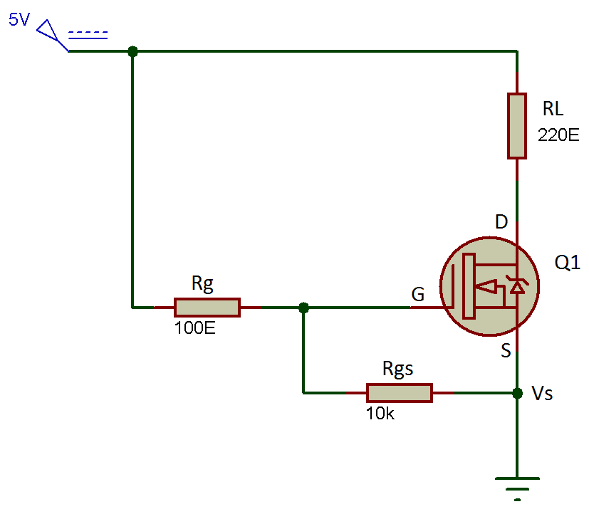
In low side switching, the source of the MOSFET is directly connected to the ground. The load (shown as resistance RL in the circuit diagram) is placed in between the drain and the power supply.
Fig. 2: Prototype of MOSFET connected as Low Side Switch
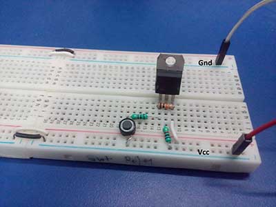
In high side switching, only the position of load is changed. In high side configuration, the load is connected between the source of the MOSFET and the ground. Since MOSFET is a voltage controlled device, for providing appropriate voltage drop at the terminals of the MOSFET, some resistors need to be connected at the gate and source of the MOSFET.
Fig. 3: Prototype of MOSFET connected as High Side Switch
While assembling these circuits, always use a gate to source resistance (Shown as Rgs in the circuit diagram) to avoid any external noise at the gate. This resistance also discharge the parasitic capacitance of the MOSFET. Otherwise, the MOSFET can get damaged as this parasitic capacitor will keep on charging and exceed the limit of the gate to source breakdown voltage. Also, do not exceed the input voltage (drain voltage and gate voltage) of MOSFET greater than its breakdown voltage as it can damage the MOSFET. A low-value resistor (10E to 500E) should be used at the gate of MOSFET. This will solve the problem of ringing (parasitic oscillations) and voltage spike in the MOSFET.
How the circuit works –
In low side switching, the load resistance is connected at the drain side of the MOSFET. As the MOSFET is a voltage controlled device, so for turning ON the MOSFET, the Gate to Source Voltage (Vgs) must be greater than the Gate to Source Threshold Voltage (Vth). In low side switching, there is no need of a gate driver circuit. In this switching mode as the source is directly connected to the ground so,
Source Voltage, Vs = 0 V
Considering gate to source threshold voltage, Vth = 4 V
So, for turning on the MOSFET, gate to source voltage (Vgs) should be greater than gate to source threshold voltage (Vth).
Vgs = Vg –Vs > Vth
Vgs = Vg – 0 > 4V
Vg = 4V
Therefore for turning ON the MOSFET, the gate voltage should be equal to 4 V. Since the applied voltage is usually 5V, this makes the low side switching process easy to implement without using any external circuitry.
Fig. 4: Circuit Diagram of MOSFET as Low Side Switch
In high side switching, the load is connected at the source side. In this configuration, When a trigger voltage is applied to the gate then MOSFET has a very low drain to source resistance i.e. Rds is very low (from milliohms to ohms depending on the type of MOSFET).
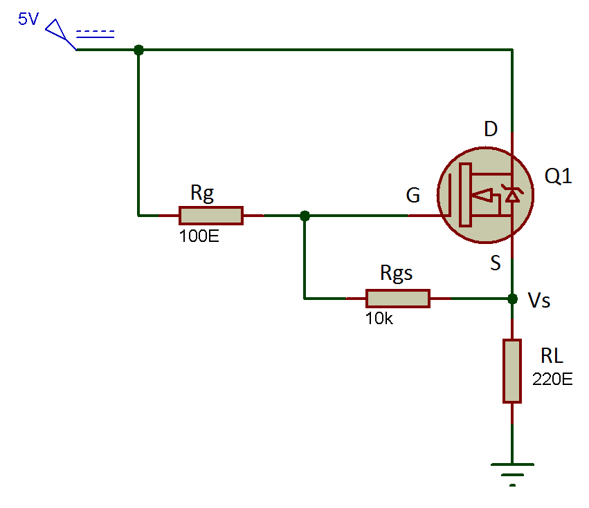
Fig. 5: Circuit Diagram of MOSFET as High Side Switch
For simplicity, the MOSFET can be represented as a resistance (drain to source resistance, Rds). Now, the voltage across the MOSFET becomes dependant on the voltage divider so formed.

Fig. 6: Simplified Circuit Diagram of MOSFET as High Side Switch
The value of Source Voltage (Vs) can be calculated in the above circuit by applying the voltage divider rule.
Voltage across Load RL, VL( or Vs) = (Vin * RL)/(Rds + RL)
Where input voltage, Vin = 5V (as commonly in circuits)
Considering Drain to Source Resistance, Rds = 10 ohms
Since Drain to Source Resistance (Rds) is very low as compared to RL, so it can be ignored in the voltage divider rule. So,
VL= Vin = 5V (approx.)
As VL= Vs
So Vs = 5V(approx.)
Considering the threshold voltage, Vth = 4V
The Gate to Source Voltage should be greater than gate to Source Threshold Voltage.
Vgs > Vth
Vgs = Vg – Vs > Vth
Vgs = Vg – 4V > 4V
So, Vg > 8V
The gate voltage should be greater than 8 V to turn on the MOSFET. But the input voltage is only 5V, that means the high side MOSFET cannot be driven by applying the same voltage at the base and drain of MOSFET. So for driving high side MOSFET, some extra circuitry is needed which can drive the gate of the MOSFET higher than the drain voltage. This extra circuitry is called Gate Driver Circuit.
There are two common methods for driving the MOSFET in high side switching –
1) Dual power supply – This method is very simple but it needs two power source. In this method, the voltage is applied at drain and gate of MOSFET by separate power supplies. So that higher voltage can be provided at the gate compared to drain of the MOSFET. This way the MOSFET can be turned ON.
2) Using Bootstrap circuit – In this method a single power source is needed, using some capacitor in the circuit. This way double or higher voltage is obtained at the gate terminal compared to the drain of the MOSFET. The capacitor in the circuit is called Bootstrap capacitor as it boost up the gate signal to a higher voltage. So by the help of the bootstrap circuit, the MOSFET can be turned ON in high side switching.
For learning more about the Bootstrap circuit, check out the following tutorial –
Driving High Side MOSFET Using Bootstrap circuit
Some manufacturers also provide specially designed ICs (commonly known as gate driver ICs) for driving the high side MOSFET. Depending on the type of IC, the IC can drive only high side or low side or it can drive high as well as low side switching simultaneously. So ICs which can drive both high and low side switching can drive the half bridge circuit, which uses one MOSFET in high side and another one in low side configuration. So for driving an H-bridge circuit (combination of two half bridge), two gate drive ICs each for driving single half-bridge need to be used. Generally, these ICs work on bootstrap technique for driving the high side MOSFET and for low side MOSFET, these simply use a transistor logic. The IR2110 IC is one of the ICs which can drive the high and low side MOSFET simultaneously.
So, the Low-side MOSFET can be turned ON without any external circuitry. But for driving the High-side MOSFET some gate driver circuit is must.
In the next tutorial, learn about testing the IR2110 IC. It is important to test the IR2110 IC before connecting it as a gate driver.
You may also like:
Project Video
Filed Under: Tutorials
Filed Under: Tutorials





Questions related to this article?
👉Ask and discuss on Electro-Tech-Online.com and EDAboard.com forums.
Tell Us What You Think!!
You must be logged in to post a comment.