Microcontrollers are purely digital devices which work on logic0 and logic1 voltages; still they are widely used for analog signal processing. There are specialized signal processors chips available which are custom made for particular applications; however a general purpose microcontroller is more than enough for small kind of signal processing applications like audio signal input and output. The microcontroller can read the analog input voltage by sampling it and converting it to their digital values. The Analog to Digital Converter (ADC) available in almost all the microcontrollers help in this task. A timer can be used to generate the sampling time period. The sampled values can then read and modify by the microcontroller. The modified signal is then output by the microcontroller in the form of Pulse Width Modulated (PWM) waves. Most of the microcontrollers have the PWM module which helps them in generating analog voltage output at an external device.
In this project PIC18F4550 microcontroller is used to read low voltage signals from a microphone amplifier circuit and try to generate the same signals which are strong enough to produce the sound in a loudspeaker. The audio signals are sampled and the same audio signals are re-constructed at the same instant from those samples in this project. The significance is that in a future project it might be possible to store the sampled values in a medium and then play the audio whenever required.
The PIC18F4550 has a built-in 10bit ADC, which is provided with a13 input channels. It has a PWM module with four output channels. In this particular project the ADC, PWM modules are used along with the timer0 modules and the method of using those modules are already discussed in previous projects. This project is actually an application which makes use of the above mentioned modules. Both the coding and the external circuitry have equal importance in this project. The working of this project can be explained with the help of the following diagram.

Fig. 2: Block Diagram of Audio Signal Generation using PIC18F4550
VOICE INPUT
The voice input block has a microphone which captures the voice signals from the surroundings. The voice signals are then amplified to a certain level using a small amplifier circuit. The amplified signal may have both positive and negative cycles. Since the ADC of the microcontroller can read only the positive voltages, the signal output from the amplifier should be clamped above the zero voltage level so that the ADC can read the complete cycle.
Hence the VOICE INPUT block is designed to capture the voice signals and modify them in such a way that the ADC of the microcontroller can read them. The following figure shows the different sub blocks inside the AUDIO INPUT block which helps to capture and modify the audio signals.

Fig. 3: Block Diagram of Audio Input Block using PIC18F4550
MICROPHONE CIRCUIT
The microphone used in this project is the commonly available condenser microphone. The microphone is pulled up using a resistor. The voice in the environment causes the capacitor plates of the condenser microphone to vibrate and hence the variation of capacitance occurs. This causes current to flow in an out of the condenser microphone according to the voice signal. The current flow produces voltage drop across the resistor which can then couple out using another capacitor.
The following image is the signal captured using CRO at the output of MICROPHONE CIRCUIT. The Volts/Division of the CRO has been set to 0.05V

Fig. 4: Output Waveform of Condenser Microphone on CRO
AMPLIFIER
The voltage signal coming from the MICROPHONE CIRCUIT is very small and hence these cannot be read by the microcontroller. Before fed this signal to the microcontroller it should be amplified. In this project a NPN transistor is used to amplify the voice signals to a particular level so that the ADC will be able to read it. Another advantage of using the amplifier is that it somewhat reduces the noise which forms along with the voice signal at the MICROPHONE CIRCUIT.
POSITIVE CLAMPER
The positive clamper is very important in this project since the ADC can read only the positive voltages and the amplified voice signals from the AMPLIFIER will be having both positive and negative cycles. The entire signal should be clamped to the positive voltage level without any distortion so that the ADC can read both the cycles. A germanium diode clamper is used in this project which can clamp the signal above a positive voltage which is equivalent to its forward bias voltage.
The following image is the signal captured using CRO at the output of POSITIVE CLAMPER. The Volts/Division of the CRO has been set to 1V

Fig. 5: Output Waveform of Germanium Diode Positive Clamper on CRO
VOLTAGE DIVIDER
The amplified signal could be sometimes larger than which the ADC can convert completely. For all the signal voltages above the ADC reference voltage the ADC will produce its maximum value only. The values which are read by the ADC are directly used to modify the pulse width of the PWM wave. Since the maximum pulse width in a PWM cycle is also limited the voltage level that is produced by the AMPLIFIER should be kept in a suitable range. The voltage divider block which consists of a variable resistor connected across the POSITIVE CLAMPER will help to keep the voltage level in a range which the ADC can read and also the pulse width of a PWM wave can represent.
TIMER
The timer module is used to generate period interrupts at a very high frequency which is well above the frequency of the audio signals. Each time the interrupt fires the value captured by the ADC is read which can be called as the sampled value of the signal at that particular instant. Thus the timer act as the sampling period generating block which samples the audio signal captured by the microphone.
The input signals should be sampled at least double the input frequency, and then only it will be possible to reconstruct the same signal. As the sampling frequency increases the number of samples increases and the reconstructed signal resembles more to the original signal. The audio signals normally fall in a frequency range from 500Hz to 5 KHz and hence the sampling frequency should be well above that frequency.
Using the timer0 module to generate sampling time is explained in a previous project on Sine wave generation using PWM module of the PIC.
ADC
The analog to digital converter (ADC) is used to convert the value of the input audio to its digital equivalent at each and every sampling period. In PIC18F4550 the digital value will be of 10 bytes long which is then used to generate the equivalent PWM wave at the output. The pictorial representation of the sample voltage generated by the ADC module at each sampling interval is shown in the following figure;

Fig. 6: Sample Voltage by ADC Module IN PIC18F4450
The Blue colored block in the above figure represents the voltage levels approximated by the ADC module on each sampling interval according to the voice signal received. The voice signal is represented by the orange colored line.
PWM
The PWM module is continuously producing a PWM wave whose pulse width can vary after each sampling time. The timer module generates the interrupt, read the ADC value and write a corresponding value to the PWM module so that the pulse width of the PWM cycles at that particular sampling time can generate the voltage at an external device which is equivalent to the voice signal at that same sampling time period.
The following figure shows the sampling of a signal voltage by the ADC module and the reconstruction of the same signal by the PWM waves. It can be noted that the reconstructed signal although not exactly same as the original signal but somewhat resembles it. As the sampling frequency increases the reconstructed signal resembles more to the original signal.

Fig. 7: Signal voltage by ADC module in PIC and Re-constructed sine wave using PWM module of PIC
The figure1 represents the sampling of an audio signal and the orange line is the signal voltage. The vertical lines shows the sampling instants at which the digital equivalent value of the signal is read into. These sample values can be then used to re-construct a wave which resembles the original wave as shown in the figure2.
The methods of generating PWM waves to produce signals are explained in a previous project on Sine wave generation using the PWM module of PIC.
VOICE OUTPUT
The voice output block converts the PWM wave to its equivalent voltage at a loud speaker. Since the loudspeaker is a device which can itself convert the PWM wave to its equivalent voltage and produce the corresponding sound, no separate filter circuit is required. This particular block mainly has a driver circuit which can drive the comparatively current consuming loud speaker with the PWM waves.
The details of the driver circuit used to drive the loud speaker according to the PWM waves are explained in a previous project on the Sound generation using PWM module of the PIC.
The following image is the signal captured using CRO at the loud speaker. The Volts/Division of the CRO has been set to 1V. The signals are not very clear due to the loading effect of the loud speaker.

Fig. 8: Output Waveform of PWM wave at loud speaker
Project Source Code
### #include#include //======================= chip config ===================// #pragma config PLLDIV = 1 #pragma config CPUDIV = OSC1_PLL2 #pragma config FOSC = HSPLL_HS #pragma config USBDIV = 1 #pragma config IESO = OFF #pragma config PWRT = OFF #pragma config BOR = OFF #pragma config VREGEN = OFF #pragma config WDT = OFF #pragma config WDTPS = 32768 #pragma config CCP2MX = ON #pragma config PBADEN = OFF #pragma config LPT1OSC = OFF #pragma config MCLRE = ON #pragma config STVREN = ON #pragma config LVP = OFF #pragma config ICPRT = OFF #pragma config XINST = OFF #pragma config DEBUG = OFF #pragma config WRTD = OFF //======================= chip config ===================// //LCD Control pins #define rs PORTBbits.RB4 #define rw PORTBbits.RB3 #define en PORTBbits.RB2 //LCD Data pins #define lcdport PORTD #define lcd_port_dir TRISD void lcd_clear ( void ); void lcd_2nd_line ( void ); void lcd_1st_line ( void ); void lcd_ini ( void ); void dis_cmd ( unsigned char cmd_value ); void dis_data ( unsigned char data_value ); void lcdcmd ( unsigned char cmdout ); void lcddata ( unsigned char dataout ); void delay_ms ( int delay ); //============================ TIMER 0 ISR =================================// #pragma interrupt tmr0_interrupt void tmr0_interrupt(void) { unsigned int v = 0; ADCON0 |= 0x02; // Start A/D conversion while ( ADCON0 & 0x02 ); // Wait until conversion gets over v = ADRESH; v = v << 8; v |= ADRESL; if ( ( v > 1 ) && ( v < 100 ) ) { CCP1CON |= ( ( v & 0x03 ) << 4 ); CCPR1L = v >> 2; } else; INTCONbits.TMR0IF=0; } //============================ TIMER 0 ISR =================================// void adc_init(void) { TRISA |= 0x01; // Configure RA0 as input pin LATA = 0; ADCON1=0x0E; // Make RA0/AN0 pin as analog pin (Other pins remain to be digital I/O) ADCON0=0x00; // Select Channel0 & ADC off ADCON2=0x80; // Right justified, 0TAD, Fosc/2 clock option ADCON0bits.ADON = 1; // Enable ADC } void main ( void ) { unsigned char data1 [] = "EngineersGarage"; unsigned char data2 [] = " AUDIO IN OUT "; int i = 0; OSCCON = 0x0C; lcd_ini (); // LCD initialization delay_ms ( 200 ); //========================= start up display on LCD ================================// while ( data1 [i] != '' ) { dis_data ( data1 [i] ); delay_ms ( 200 ); i++; } i = 0; lcd_2nd_line (); while ( data2 [i] != '' ) { dis_data ( data2 [i] ); delay_ms ( 200 ); i++; } i = 0; //========================= start up display on LCD ================================// //============================ PWM SETTINGS ====================================// TMR2 = 0x00; // setting TMR2 value as 0, start counting from 0 PR2 = 22; // set the PR2 value, to get PWM period of 2us CCPR1L = 0x00; // setting initial value of CCPR1L as 0 CCP1CON = 0x0C; // select single output with P1A, and mode select bits so as to get P1A, P1B, P1C and // P1D as active-high TRISC &= 0xFB; // setting the PWM pin as output T2CON = 0x04; // both the pre-scalar and post-scalar bits are written for 1:1 with the timer2 turned on. INTCONbits.T0IF = 0; // turning off the Timer0 interrupt TMR0L = 0xFE; // setting the timer register to value T0CON = 0xC0; // enable the timer, select the timer in 8bit, select CLKO, assign the pre-scale value 1:4 INTCONbits.TMR0IF=0; // clearing the timer0 overflow bit INTCONbits.T0IE = 1; // enabling the timer0 interrupt INTCONbits.GIE = 1; // enabling the global interrupts //============================ PWM SETTINGS ====================================// adc_init (); while ( 1 ) { ; } } //======================== LCD routines defenitions ========================// void delay_ms ( int delay ) { int ms, i; for ( ms = 0; ms < delay; ms ++ ) for ( i = 0; i < 70; i ++ ); } void lcd_ini ( void ) { TRISB &= 0xE3; lcd_port_dir &= 0x0F; dis_cmd ( 0x02 ); // to initialize LCD in 4-bit mode. dis_cmd ( 0x28 ); //to initialize LCD in 2 lines, 5X7 dots and 4bit mode. dis_cmd ( 0x0C ); dis_cmd ( 0x06 ); dis_cmd ( 0x80 ); dis_cmd ( 0x01 ); delay_ms ( 500 ); } void dis_cmd ( unsigned char cmd_value ) { unsigned char cmd_value1; cmd_value1 = cmd_value & 0xF0; //mask lower nibble because PA4-PA7 pins are used. lcdcmd ( cmd_value1 ); // send to LCD cmd_value1 = ( ( cmd_value << 4 ) & 0xF0 ); //shift 4-bit and mask lcdcmd ( cmd_value1 ); // send to LCD } void dis_data ( unsigned char data_value ) { unsigned char data_value1; data_value1 = data_value & 0xF0; lcddata ( data_value1 ); data_value1 = ( ( data_value << 4 ) & 0xF0 ); lcddata ( data_value1 ); } void lcdcmd ( unsigned char cmdout ) { lcdport &= 0x0F; lcdport |= cmdout; rs = 0; rw = 0; en = 1; delay_ms ( 50 ); en = 0; delay_ms ( 50 ); } void lcddata ( unsigned char dataout ) { lcdport &= 0x0F; lcdport |= dataout; rs = 1; rw = 0; en = 1; delay_ms ( 50 ); en = 0; delay_ms ( 50 ); } void lcd_clear(void) { dis_cmd(0x01); delay_ms(10); } void lcd_2nd_line(void) { dis_cmd(0xC0); delay_ms(1); } void lcd_1st_line(void) { dis_cmd(0x80); delay_ms(1); } //======================== LCD routines defenitions ========================// ###
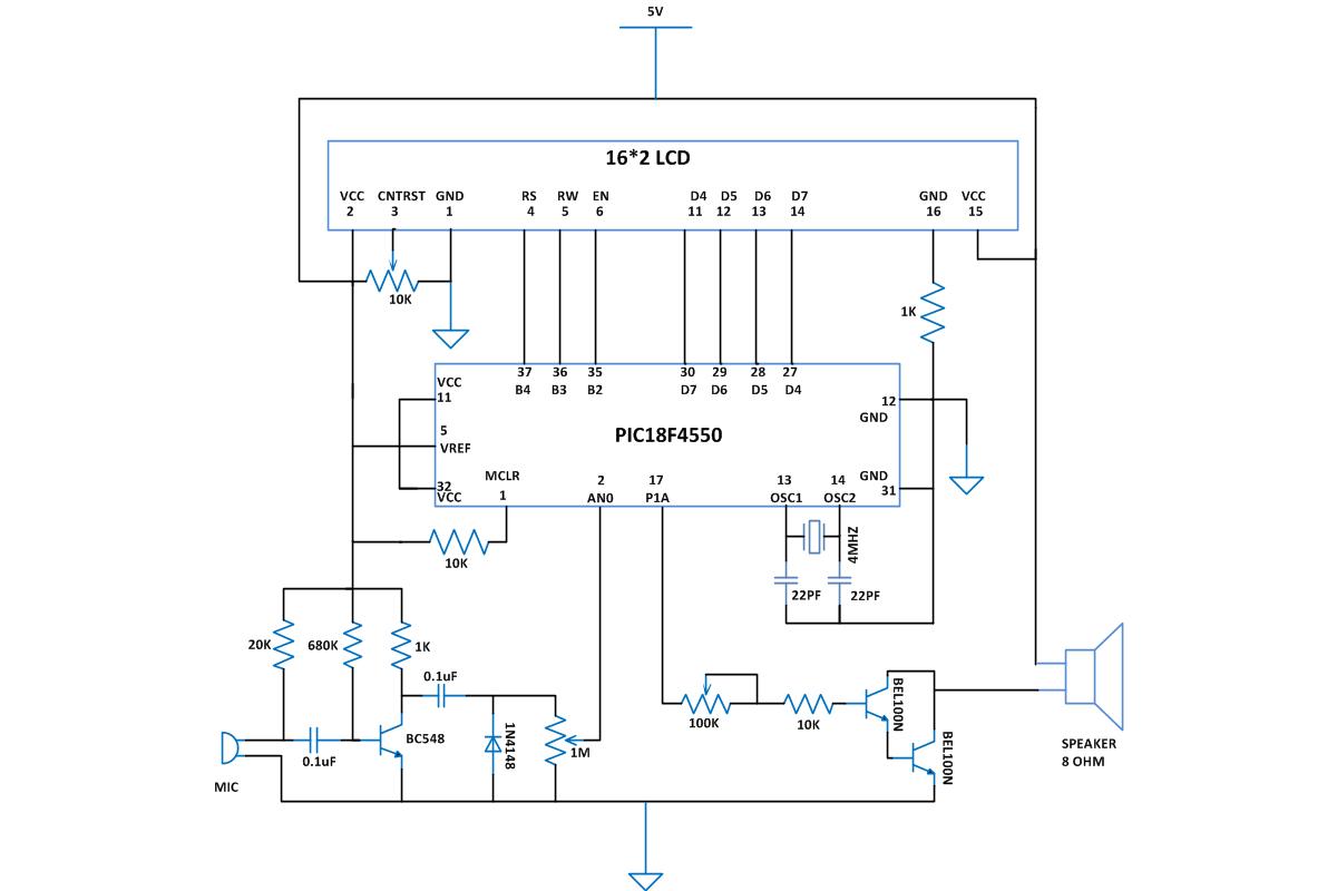
Circuit Diagrams
Project Components
Project Video
Filed Under: PIC Microcontroller.
Filed Under: PIC Microcontroller.

Questions related to this article?
👉Ask and discuss on Electro-Tech-Online.com and EDAboard.com forums.
Tell Us What You Think!!
You must be logged in to post a comment.