PCB Design – KiCad library Editor:
When we are designing a PCB in any CAD software, we need to find suitable components. Like, if we need resistor, we must be clear about component type, dimensions (optional), SMD component or through hole component, and different parameters. Any EDA software consists of components libraries. We can select a required component from library, but the library may not have all the components. If we need any component which is not present in the library, then we need to create and save it in the library so as to use it in future. In KiCad, we can use library editor to create a new component. Library editor is a part of Eeschema.

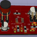
Fig. 1: Screenshot of KiCad PCB Design Tool
Note: Before editing and creating new component, create a new folder in the project folder named library. In this file we can put all our newly created components.
Before creating a component we need to gather sufficient details about component, like pin diagram, pin configuration, its size, shape, dimension etc. So before starting library editor, go though the component data sheet.
In this tutorial, I am choosing CD4017 IC. Moreover, for pin diagram, pin configuration and other required details, I have referred our website engineersgarage.com. Required information about component: http://www.engineersgarage.com/electronic-circuits/understanding-decade-counter-cd4017
After this step, open library editor in Eschema, a new window will appear on the screen. In this window, we can see the required tools to edit component at the right edge of the window.
To start editing, click on “create new component” option.

Fig. 2: Screenshot of Creating New Component on KIcad
A new window will appear on the screen. Enter the component name in Empty field, select required changes in remaining options, and click on “OK”.

Fig. 3: Screenshot of Component Properties Window on KIcad
The name will be placed at the middle of the work sheet. Move it from there and place it at the top of the component. Now select the “Place pin” option and left click on work sheet. “Pin properties” window will appear on screen. In this window, we have to give the name of the pin, number of the pin, Orientation of the pin and Electrical type of the pin.
Note: Specify the pin number and name as per pin diagram. Also follow the diagram for pin orientation. Select electrical property of the pin as pin description (INPUT, OUTPUT, BI-DIRECTION etc.) in data sheet. Selecting Electrical type of the pin is very important, please do not neglect it. Select perfectly, or else there will be errors after ERC.
After placing all pins with their names and numbers, choose “Add graphic rectangular to component body” and draw the rectangle touching all pins.

Fig. 4: Graphical Image of a Component

Fig. 5: Screenshot of Component Placed on Layout in KIcad
After creating CD4017, save it in a new folder meant for library components (if any).
After saving this, close the editor and open the Eeschema circuit editor. Then click on Add components option and search for the created component (CD4017). If it is found, place it on worksheet. Else directly open the created library folder and select the component from there.
You may also like:


Filed Under: Featured Contributions, Tutorials

Questions related to this article?
👉Ask and discuss on EDAboard.com and Electro-Tech-Online.com forums.
Tell Us What You Think!!
You must be logged in to post a comment.