Most of the modern devices are run by the batteries. A battery stores the charge and then supply that charge to power up any electronics device. Though batteries are handy to use, their use need some precautions too. A major problem with the use of batteries is their over discharging and over charging. Both of these issues affect the life of a battery and cost the end user needlessly. These issues are often ignored by the users too. The improper handling of batteries shorten their life and may even lead to explosion. This ultimately increases the maintenance cost of the electronics devices.
In this electronics project, a zener diode based circuit will be designed to protect a battery from over charging. When a battery is charged, its terminal voltage i.e. voltage between the anode and cathode of the battery increases. On full charging, the terminal voltage reaches a peak value which is an indication of 100 percent charging. Charging a battery beyond its full level leads to permanent or temporary damage of the battery.
It is possible that over charging can cause battery to lose ability to recharge again or even the battery can explode due to overcharging. The percentage or level of charging of a battery is therefore estimated by its terminal voltage. The battery must be disconnected from the charger circuit once the peak terminal voltage is detected or the battery is once fully charged Therefore, there should be a protection circuit which can monitor the level of charging of the battery by detecting the terminal voltage and protect the battery from over-charging by cutting off the battery connection with the charger.
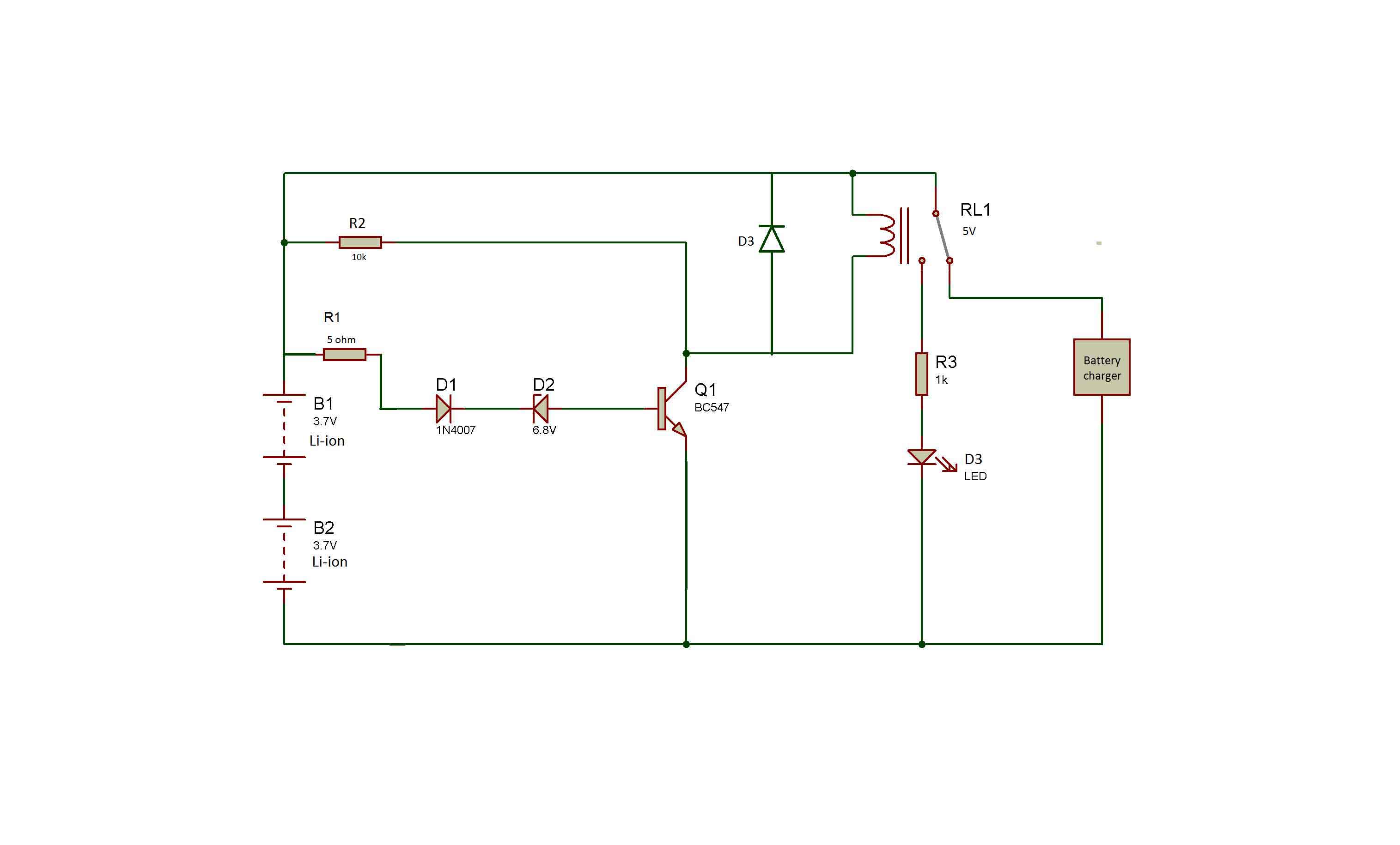
In this electronics project, a power circuit is designed which will detect the upper limit of the terminal voltage by the use of a suitable Zener diode and will cut off the battery connection with the load device by the use of a relay. The circuit includes an LED indicator section also which will light up the LED as the battery charges to peak value and does not require recharging.
Specifically, in this project two Li-ion batteries connected in series will be taken as power supply unit. In most of the commonly used portable electronics devices like laptops, smart phones and others, the Li-ion batteries with 4.2 V of peak limit of the terminal voltage are used. Since in this project, batteries with cut off limit of 4.2 V are used for power supply, so, using two batteries in series set the cut off limit to 8.4 V. Practically, the protection circuit designed in this electronics project cuts off the battery from the charger when the battery voltage goes beyond 8.37V.
So, a zener diode circuit having a drop of 8.4 V in reverse bias condition is used to detect the cut off limit in the design of the circuit. The Zener circuit can be designed multiple ways. A single zener diode can be used or a combination of zener diodes can be used to attain the desired voltage drop in reverse bias condition. Another option is to use a normal diode in combination with the zener diode which is used in this project. The diode circuit will be used to drive a switching transistor which will operate the relay.
As the terminal voltage of the battery will go above the 8.4 V, the diode circuit will go in conduction state, triggering the switching transistor and changing the relay state to cut off the supply from the charger. After understanding the functioning of this project, protection circuits for other cut off limits can also be designed by proper selection of the zener diode and relay with the same circuit.
Components Required

Fig. 1: List of Components required for Battery Overcharging Protection Circuit with Automatic Cut Off
Block Diagram –

Fig. 2: Block Diagram of Battery Over Charging Protector
Circuit Connections –
The circuit designed in this project has the following circuit sections –
1) Zener Diode Circuit for detecting cut off terminal voltage of the battery
2) Transistor circuit to operate the relay
3) Diode circuit for back current protection
4) LED indicator circuit for indication of full charging of the battery
1) Zener diode circuit – The Zener diode circuit can be built multiple ways. Let us consider three ways to design the zener diode circuit –
a) By taking a zener diode equivalent to the desired cut in voltage – Since the zener diode circuit will be used to trigger a switching transistor, the voltage drop across the transistor is must to consider. A single zener diode having the peak reverse voltage equivalent to desired voltage drop minus voltage drop across the switching transistor circuit can be taken. In this way the rating of the required voltage drop can be calculated in the following manner –
Cut in voltage, Vcut = 8.4 V
Vcut= voltage drop across Zener diode (D1) + Voltage drop across transistor (Q1) (Vbe)
8.4 = voltage drop across Zener diode (D1) + 0.7
Voltage drop across Zener diode = 8.4 -0.7
Voltage drop across Zener diode = 7.7 V
So for a cut in voltage of 8.4 V, a zener diode of 7.7 V rating should be selected.
b) By taking combination of zener diodes – Since the voltage drop across the zener diode circuit should be 7.7 V. So if a zener diode of exact 7.7 V peak reverse voltage rating is not available then a combination of zener diodes connected in series can be used. For example, two zener diodes with 3V and 4.7 V rating can be used.
c) By using normal diode with zener diode – The voltage drop across the zener circuit can be matched to 7.7 V by connecting a typical diode in forward bias in series with the zener diode. For example, a zener diode of 7 V can be used in series with a 1N4007 diode. The 1N4007 diode has forward voltage drop of 0.7 V so it will provide the extra 0.7 V drop. This will make the exact 7.7 V which is the required cut in voltage in the circuit. The same method is used in the design of this battery over charging protection circuit.
The regular diode is connected in forward bias configuration with its anode connected to the anode of the battery and cathode connected to the cathode of the zener diode. The zener diode is connected in series with the normal diode in reverse bias configuration with anode connected to the base of the switching transistor and cathode with the cathode of the normal diode. Until the terminal voltage of the battery will be below cut off limit and the peak reverse voltage of the zener diode, the zener diode will remain in non-conduction state but as the terminal voltage will rise above cut off and the peak reverse voltage of the zener diode, it will go in conduction state.
2) Transistor circuit – The transistor circuit is used to operate the relay. A switching transistor is used as high side switch in the circuit where the transistor is operating as logical inverter. The anode of the zener diode is connected to the base of the transistor Q1, the emitter of the transistor Q1 is connected to ground while collector of the transistor is connected to the relay coil which controls the supply from the battery charger.
3) Diode Circuit – A diode circuit is connected parallel to the relay coil for back current protection from the relay. The back current from the discharging of the relay coil can permanently damage the battery that is why, this diode circuit is used for back current protection.
4) LED indicator circuit – The LED indicator circuit is connected at the NC point of the relay. When the transistor circuit switches the relay to NC point, the LED gets forward biased as the anode of the LED is connected to the NC point of relay and cathode is connected to ground. A current limiting resistor is connected in series with the LED to avoid any damage to the LED by excessive voltage.
How the circuit works –

Fig. 3: Prototype of Battery Over Charging Protector designed on a breadboard
The circuit is based on the working of zener diode. A zener diode when connected in reverse bias configuration and its cathode voltage is below its breakdown voltage then zener acts like an open circuit. But when a voltage above zener breakdown is applied at its cathode terminal then zener starts conducting from the cathode to anode in reverse bias condition. As the zener diode can also work in reverse bias, this feature of zener diode is useful for detecting the cut in voltage level of the battery.
There are two Li-ion batteries connected in series so they have a total 8.4 V peak terminal voltage. When the two Li-ion batteries will be connected with the charger then there can be two cases as follow –
The Terminal Voltage of Battery can be below 8.4 V- When the battery voltage is below 8.4 V then the cathode of the zener diode (D1) will be below 6.8 V. The diode D1 will start conducting and there will be drop across D1 and Q1. In this case, zener diode will remain in non-conduction state and will not conduct current from cathode to anode terminal (as shown in below image). As the base of Q1 transistor is connected to the anode of zener (as shown in below image). So the base of transistor Q1 will not get the required voltage and it will act like an open circuit. So the transistor Q1 is working as a logical inverter. When the zener diode is in non-conduction state and there is not sufficient voltage at the base of the transistor, the collector current is short circuited to ground through emitter and collector voltage is dropped.
Practically it is observed that although zener below 8.25 V will not conduct but still it has some current (in microamperes) which flow from its cathode to anode, this current is the leakage current of the Zener.

Fig. 4: Circuit Diagram showing Zener Diode Section of Battery Over Charge Protector
Generally, as the current at the transistor base start increasing it acts like a variable resistance, the value of this resistance start decreasing as current increases. Considering BC547 transistor, the voltage across the base to emitter is in between 0.65 V to 0.7 V then the transistor will act as a short circuit. The transistor (BC457) has a minimum gain of 110 so the base of the transistor needs a very less current to conduct. So, the transistor Q1 will amplify the microamperes leakage current in milliamperes and current in milliamperes will start flowing from collector to emitter (As shown in below image). So, the leakage current from Zener will also switch ON the transistor Q1. But in this state, the Q1 is not fully ON as the base to emitter till now not reaches to 0.65 V.

Fig. 5: Circuit Diagram showing High Side Switch working in Battery Over Charge Protector
The collector of the transistor Q1 will provide ground to the relay (RL1) so that the relay can be activated. But in this case, as the Q1 is not fully ON so there will be some voltage drop across collector to emitter of the transistor Q1. Hence in this case relay will not activate and the battery will remain in charging state through the charger. The output LED also remains in off state (as shown in below image).

Fig. 6: Circuit Diagram showing Practical High Side Switch working in Battery Over Charge Protector
The other case can be when the Terminal Voltage of Battery can be below 8.37 V. When the battery voltage will above 8.37 V, the diode D1 will start conducting and the zener diode will break down. So in this state zener diode will allow the current to flow from its cathode to anode terminals (as shown in below image).

Fig. 7: Circuit Diagram showing Zener Diode working in Battery Over Charge Protector
As the base of Q1 transistor is connected to the anode of zener (as shown in below image). So the transistor Q1 will start conducting and act like a short circuit. Therefore, all the collector current of Q1 will get a shorted path and start flowing from collector of Q1 to its emitter, finally to ground.

Fig. 8: Circuit Diagram showing Relay operation in Battery Over Charge Protection
So the voltage difference of collector to emitter is zero since all the current drains to the ground. This will activate the relay. Therefore, the charger which is at NC(normally closed) pin will disconnect from the battery. The LED at the NO (normally open) pin of the relay lights up and will indicate the over charging of the battery.

Fig. 9: Circuit Diagram showing complete working of Battery Over Charge Protection
Use of series resistance(R1) with Zener diode and with other components
A Zener diode requires a series resistance which limits the flow of current through it above its current rating, this will prevent the Zener diode from overheating. With the use of series resistance, Zener can also provide a regulated voltage at the output. A resistance R2 is connected to the collector of transistor Q1 and resistance R3 is connected to the LED. The purpose of these resistances is just to limit the current from the transistor and the LED. This will prevent the components from any damage.
Selecting Zener diode Series Resistance (R1)
In this project, the zener diode used has 6.8 V rating. When the voltage will exceed 8.4 V then the circuit will cut off the battery from charger. Although the increase in voltage is very less but to be on safe side maximum voltage cut off can be taken 8.5 V. The series resistance of the zener diode can be calculated by the following equation –
R1 = (Vs-Vz)/Iz
Where Vs = maximum supply voltage
Vz = (Total voltage across zener(D2) +1N4007 diode(D1)+ drop across zener resistance(R1)+ transistor(Q1))
Iz = Zener current
For calculating value for resistance R1, the Zener current can be calculated by the following method –
Maximum Power dissipation of Zener diode, Pz = 250 mV
Vz =8.4 V
Maximum Zener current, Iz can be calculated as follows
Pz = Vz * Iz
Iz = Pz / Vz
Iz = 0.25/8.4 V
Iz = 29 mA (approx.)
Now by above equation resistance can be calculated as
Vs = 8.5 V
R1 = (Vs-Vz)/Iz
R1 = (8.5-8.4)/0.029
R1 = 3.5 ohms (approx.)
But in the experiment, the resistance R1 is taken 5 ohms just to be on safe side. The selection of zener series resistance must be chosen wisely so that it will not allow current more than the zener rating. As more current will permanently damage the zener diode.
The different voltage readings taken from the circuit are summarized in the following table –

Fig. 10: Table listing different voltage readings taken from the circuit
The verification of the practical value of the cut in voltage of the can be determined by the drop across the other components by using the following equation –
Practical observation,Vcut = voltage drop across Zener diode (D2) + Voltage drop across transistor(Q1) (Vbe) + voltage drop across series resistance (R1)+ voltage drop across diode(D1)
In above equation, on adding the diode(D1) drop also which is not there in the theoretical observations
Practical observation,Vcut= 6.8 + 0.68 + 0.2 + 0.69
Practical observation,Vcut= 8.37V
From the above practical observation, it is can be analyzed that the practical voltage at which the battery disconnects from the charger is 8.37 V. Therefore, the battery will cut off when the battery voltage of each Li-ion battery is at 4.2 V approximately.
Use of diode (D3)
As internally the relay has an inductor coil this coil stores some charge when the relay gets activated or energized. When relay gets de-energized then the polarity of the relay gets reversed and a back current will flow from the coil, this may damage the circuit. Therefore a diode (D3) is used across the relay to prevent the circuit from the back current when the relay is de-energized. This diode is known as fly back diode or freewheel diode. The inductor will discharge through this diode and this will prevent the other circuitry from any back current.
It is important that the relay voltage rating should be less than the cut-off voltage of the battery. For e.g. if in the circuit, a 9V relay is used then it will never get energize at 8.4 V. That is why 5V relay is used in the circuit.
You may also like:


Circuit Diagrams
Filed Under: Electronic Projects

Questions related to this article?
👉Ask and discuss on Electro-Tech-Online.com and EDAboard.com forums.
Tell Us What You Think!!
You must be logged in to post a comment.