Flash Memory is a non-volatile form of computer memory that remembers all the information even when the device is switched off. In this, the user can electronically erase or reprogram the data as and when required. Although it was introduced for the first time back in the 1980s, the usage has witnessed a rapid increase in the last few years. This is because the production of portable and technologically advanced devices has grown enormously and almost all of these devices are fitted with flash memory.
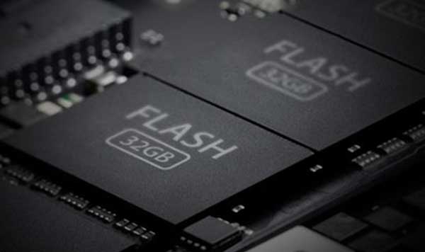
Nowadays we can find the real-life application of flash memory in so many devices surrounding us. These include USB memory sticks, digital cameras, MP3 players, and smartphones and so on. As we can see around us, the memory cards are the most common forms of flash memory available in the mass market. These have become the latest mediums used for storing and transmitting data among the hi-tech devices. There are different categories of these cards depending upon their applications and capacity.
Here we are going to talk about the basic concept of Flash memory along with all the important details like its working, types and lifecycle.
What is meant by Flash Memory?
There are two kinds of computer memory namely RAM (Random Access Memory) and ROM (Read-Only Memory). The former remembers everything as long as the computer’s power is kept on whereas the latter are already stored with necessary information and hence these don’t forget any information. A computer needs a combination of both these, which is why hard drives are used. These drives make use of a combination of RAM and ROM chips thereby storing information that is remembered for an indefinite time period, whereby the user can read and write the data.
Similarly, the portable and small-sized devices like MP3 players and digital cameras are equipped with flash memory. These memory cards reflect a mixture of both RAM and ROM features in a way that these can store data for an indefinite time period and the data can be re-written or erased as per the needs.
Types of Flash Memory
There are mainly 2 types of Flash memory depending upon the applications. The technology utilised in both these categories is similar but the approach for reading and writing the data is different. Let’s have a look at these -:
• NAND Flash Memory
NAND flash architecture was introduced by Toshiba in 1989 for addressing the need for a lower cost per bit and higher performance. It offers high cell densities implying a large storage capacity along with fast write and erase rates. Besides, the system interface is quite consistent which eases upgrades; however, it has special requirements too.
• NOR Flash Memory
Nor flash chip was introduced by Intel in 1988 which proved to be a suitable replacement for ROM chips. With NOR, users can run an application directly from flash instead of making use of the application code into system RAM. A Higher level of software for NOR is offered by several popular vendors like Microsoft and Intel. It is highly cost effective for lower capacities i.e. 1-4 Mbytes and delivers high read performance but lacks speed in the write-and-erase functions.
Working of Flash Memory
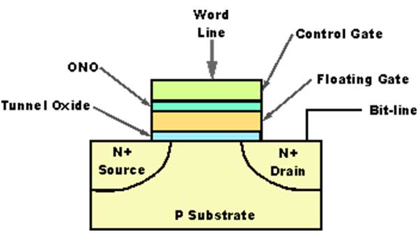
To understand the working of Flash Memory, let’s first check out how a transistor works. A regular transistor is similar to a pipe through which electricity flows like water. Its two ends are called source and drain and there is a gate in between which blocks electricity. When the power is on, the gate is open and electricity flows freely, storing one. But when the power is turned off, the gate also closes and blocks the flow of electricity, storing zero. Now next time when the power is switched on, the gate remains closed and that’s why it fails to retain the information.
You may find useful to read about: Beginner’s Guide to Electronics
In flash memory, the transistor has two gates namely- control and floating. The two ends i.e. source and drain are rich in electrons but are separated by a p-type material which is electron deficient. So, in order to allow the electrons to flow freely between the two gates, a positive voltage is applied to the contact points (word line and bit line) which pull the electrons in a rush. During this, some electrons get trapped between the control and floating gate. Now even when the power is switched off, the leaked electrons stay there for an indefinite period of time. Hence, it is able to retain all the data whether the power is switched on or off.
Programming of Flash Memory
Earlier, programming Flash memory was quite difficult because of the limited number of erase programme cycles. They used to carry a few hundred cycles mainly because of the destructive breakdown of the thin gate oxide layer. However, with time, improvements were made to improve the quality of the oxide layer which in turn helped in enhancing the life of the flash memory. Now the chips are programmed without worrying about the life span or the number of programme cycles.
Flash Memory Wear Mechanism
As mentioned above, the life span of flash memory is of a great concern for ensuring that the stored data is not lost. This wear out happens mainly because the oxide layer starts to degrade with usage over a long period of time. The processes used for programming and erasing the cycle of Flash memory are termed as hot-electron injection and tunneling respectively. This not only degrades the erase characteristics but also leads to the closure of memory cell threshold window.
Dealing with the Wear out of Flash Memory
In order to solve the problem of limited erase cycles and limited life span, there is a procedure called wear leveling. The main aim behind this is to track the used blocks and then distribute the programme and erase cycles evenly across the memory. This helps in avoiding the excessive use of blocks and their pre-mature failure. There are three ways to deal with this issue, described below -:
• No wear Levelling
In this, the logical addresses from the operating systems from the operating systems to the memory’s physical address. When there is a change in the location, the content of that block is erased and re-programmed. This is very time-consuming and doesn’t help much in solving the wear out the problem.
• Dynamic Wear Levelling
In this approach, a map is used to link the logical addresses of the OS with the physical location of flash memory. When new data is written, the original block is marked invalid and the map is linked to a new block. It’s called dynamic because it only recycles the changed data while the old blocks are marked invalid and left unused.
• Static Wear Levelling
It is the most effective approach among the two mentioned above. It’s similar to the dynamic method except that it moves the unchanged i.e. static data periodically and hence levels the usage of cells across the whole memory.
Applications of Flash Memory
Flash memory can be found in almost all the portable devices around us. Basically, there are three forms which are quite common nowadays. These applications are described below -:
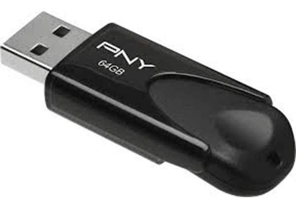
• USB Flash Drive
We also recommend: USB- an Overview
These devices are popularly known as pen drives and contain flash memory with an integrated USB interface. The data enclosed in such devices is removable and rewritable. The maximum storage capacity carried by a USB drive is up to 2TB are being planned. These have replaced the floppy disks as they have more storage capacity and transfer data at a much faster rate.
• Memory Card
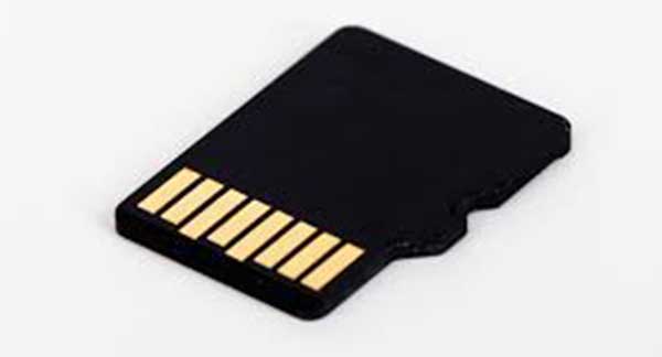
The memory card is a storage device that is used in almost every device nowadays including mp3 players, mobile phones, laptops, digital cameras and video game consoles. This form of flash memory has evolved from compact flash cards back in 1994 to the postage stamp-sized Secure Digital Cards in 2001. Nowadays we can find the latest miniSD and microSD cards that are fitted with higher storage capacities and work faster.
• SSD Card

SSD, also known as Solid State Drive/Disc, is the latest form of flash memory that has replaced hard drives in the computers. Since there is no moving part involved, the chances of mechanical failure are negligible. These are much smaller in size, consume less power, run cooler and yet respond at a much faster rate. The demand for SSDs is driven by the need for higher I/O performance. These have lower random and read access latency, which makes them fit for heavy workloads.
You may read our blog and article section for more topics on electronics engineering, industry, and technology.
Filed Under: PIC Microcontroller., Tech Articles

Questions related to this article?
👉Ask and discuss on Electro-Tech-Online.com and EDAboard.com forums.
Tell Us What You Think!!
You must be logged in to post a comment.