Pulse Width Modulation (PWM) is a technique in which the width of a pulse is modulated keeping the time period of the wave constant. The ON time and OFF time can have any different values in the wave cycles, but the sum of the ON time and OFF time remains same for the entire cycles.
This feature of the PWM wave is making use in so many digital systems like DC motor control, audio devices, simple decoration light controls etc. The PIC18F4550 has an inbuilt PWM module which can generate continuous PWM waves. This project explores the PWM module of the PIC18F4550 and tries generating a sine wave with the help of a filter circuit.
The PIC18F4550 has four PWM output channels and they are P1A, P1B, P1C and P1D. All of them are capable of generating PWM waves at a time. In this project only one of the PWM channels are using. The P1A is the PWM channel in this particular project. A simple example of the of waves generated at this pin is shown below;
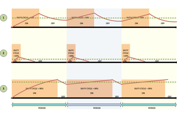
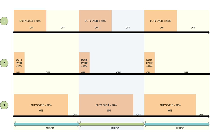 As shown in the above figure the ‘Period’ of all the wave remains the same but their ‘Duty-cycle’ varies.
The period of the wave is the sum of the ‘ON time + OFF time’. Duty-cycle is the percentage of time period for which the logic1 voltage exists in a cycle (ON time), starting from the beginning of the cycle.
The PWM is that kind of a wave in which the ON time and OFF time can vary in a cycle but the sum of ‘ON time + OFF time’ remains constant for every cycle.
The period and the duty cycle for a PWM wave can be calculated generally using the following equations;
Period = ON time + OFF time
Duty-cycle = ON time / (ON time + OFF time) = ON time / Period
As shown in the figure, the first PWM wave has a Duty-cycle of 50% which means the on-time is exactly half of that the period of the wave. The second wave has 10% Duty-cycle and the third wave has 90% Duty-cycle.
According to the modulation of the width of a pulse in a period of the wave, the PWM can generate any required voltage with the help of a proper filter circuits. The filter circuits are used for generating the voltage corresponding to a modulated wave. Hence the PWM wave is always associated with a filter circuit. When applied to a proper filter the 50% duty cycle can produce half of the maximum voltage of the pulse. If the maximum voltage (logic 1 voltage) of the pulse is 5V then the 50% duty cycle wave can produce a continuous 2.5V. The 10% duty cycle wave can produce nearly 0 voltages and the 90% duty cycle wave can produce nearly 5V.Thus the wave when applied to a filter can continuously produce a voltage which is the average of the voltage in a single period.
Increasing the Duty-cycle will increase the voltage at the filter device’s output and decreasing the Duty-cycle will decrease the voltage as well
 The filter could be any device which can generate the equivalent voltage of a PWM wave. It normally consists of Low-pass filters, amplifiers, load drivers etc. They generate the voltage corresponding to the pulse width modulation in the wave and can fed that voltage to the load device. The registers associated with the PWM modules like CPR1, PR2 and TMR2 etc. can be used to set the required Period and Duty-cycle in a PWM wave.
The voltage generated by the PWM wave at a filter device can vary by simply varying the Duty-cycle of the PWM wave. Increasing the Duty-cycle will increase the voltage at the filter device’s output and decreasing the Duty-cycle will decrease the voltage as well. In this particular project the sine wave samples are generated periodically by re-writing the value of the CCPR1 register to vary the Duty-cycle. It is done by generating interrupts periodically with another timer module timer0 and changing the CCPR1 value when the code is inside the timer0’s ISR. It is done as shown in the following figure;
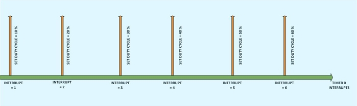
The voltage generated by the PWM wave in the interval between two interrupts will be a constant value and this time period can be called ‘sampling period’.
The values of voltage that appears at each sampling period are simply called ‘samples’.
A sampling time can have 10 to 500 PWM cycles normally and depends on the particular output device requirement.
The more the number of PWM cycles in a Sampling time, more stable the output voltage will be
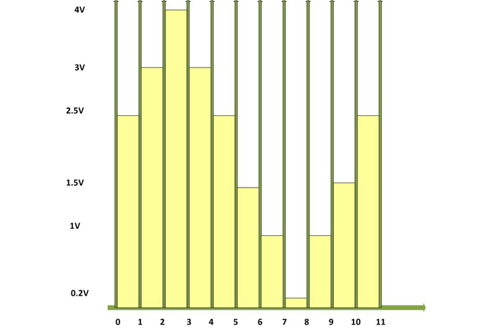
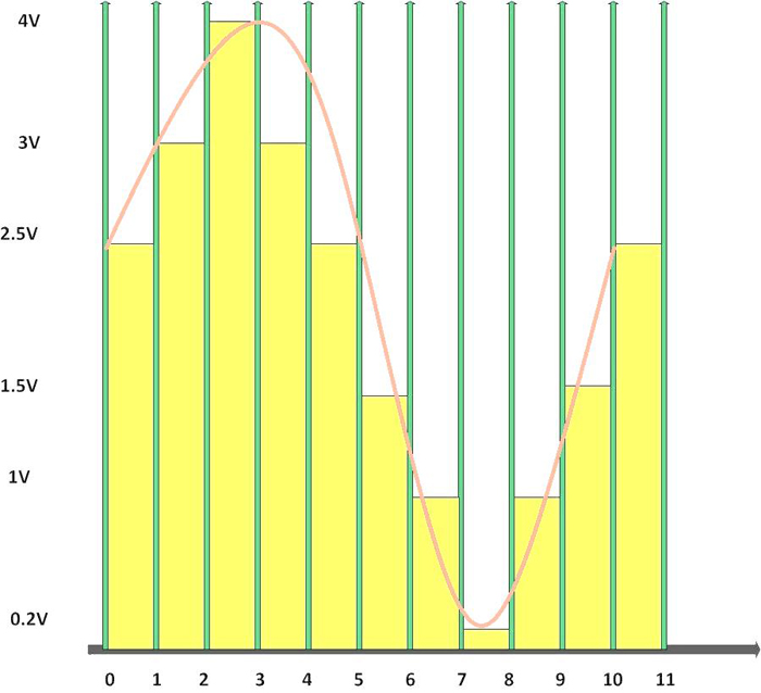
The Duty-cycle of the PWM wave is increased in a sinusoidal way each times the timer0 fires and to perform such a thing one has to configure the timer0 properly. The consecutive samples that should be generated at each sampling time should follow a sinusoidal pattern. These samples should have the values as if they have been taken by sampling a real sine wave. An example of the sine wave samples is shown following figure in which 10 samples are used to resemble a sine wave.
These values when applied to a filter circuit can generate the sine wave at its output by smoothing the step size. The output of the filter which is fed with the sine wave samples is shown in the following figure. The brown line shows the actual sine wave constructed by the filter circuit.
The values that should be assigned to the CCPR1 register to generate such consecutive samples are actually taken from a look-up table. The look-up table with 50 samples which is used in this particular project to generate the sine wave is shown in the following;
|
Sample no. |
Value |
Sample no. |
Value |
Sample no. |
Value |
Sample no. |
Value |
Sample no. |
value |
|
1 |
52 |
11 |
85 |
21 |
69 |
31 |
28 |
41 |
16 |
|
2 |
57 |
12 |
86 |
22 |
65 |
32 |
25 |
42 |
18 |
|
3 |
62 |
13 |
86 |
23 |
61 |
33 |
22 |
43 |
20 |
|
4 |
66 |
14 |
86 |
24 |
56 |
34 |
19 |
44 |
23 |
|
5 |
70 |
15 |
85 |
25 |
52 |
35 |
17 |
45 |
26 |
|
6 |
74 |
16 |
83 |
26 |
48 |
36 |
15 |
46 |
39 |
|
7 |
77 |
17 |
81 |
27 |
44 |
37 |
14 |
47 |
34 |
|
8 |
80 |
18 |
78 |
28 |
39 |
38 |
14 |
48 |
38 |
|
9 |
82 |
19 |
75 |
29 |
35 |
39 |
14 |
49 |
43 |
|
10 |
84 |
20 |
72 |
30 |
31 |
40 |
15 |
50 |
48 |
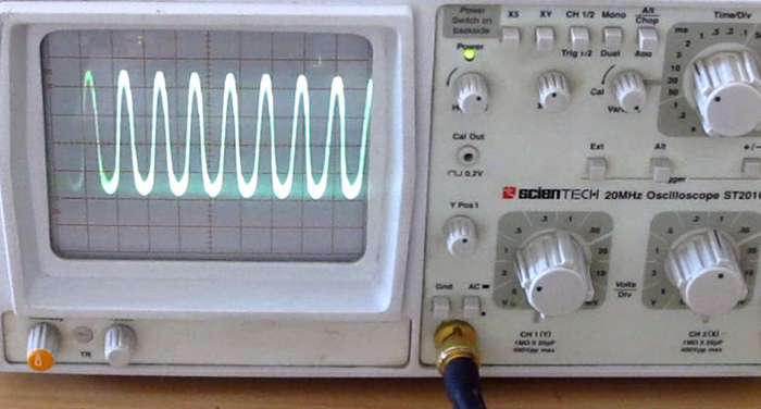
When these values are assigned to the CCPR1 at consecutive sampling periods, it can generate a sine wave at the output of the filter circuits. A zoomed in image of the sine wave that has been generated by the filter used in this project using the above look-up table is given in the following. The sample step value creating the sine wave can be seen in this image.
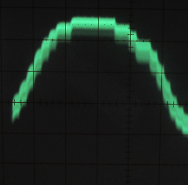 The steps are not very clear and it should not be since the capacitor in the filter circuit smoothed out the steps to create the sine wave.
Time period calculations:
Sampling time:
In this project the TMR0 is set to zero and the timer0 is configured as an 8 bit timer with pre-scale value 1:2. Now the timer will count from 0x00 to 0xFF with a clock frequency of FOSC/4 with a pre-scale of 1:2.
The CPU clock frequency is set as 48MHz and hence the time period of a single clock TOSC can be calculated as
TOSC = 1/ FOSC = (1 / (48*10^-6) = 0.02 * 10^-6 seconds.
The time period of the clock which the timer0 module receives can be calculated as
1 / (FOSC/4) = TOSC * 4 = (0.02 * 10^-6) * 4 = 0.08 * 10^-6 seconds.
The timer0 has a pre-scale value of 1:2 and hence the time period should be again multiplied by 2.
Hence the time period at which the value in the 8 bit timer increases = (0.08 * 10^-6) * 2 = 0.16*10^-6 seconds.
The timer0 value increases from 0x00 to 0xFF with a time period of 0.16*10^-6 seconds.
Hence the total time taken for the timer to overflow and cause an interrupt can be calculated as
0.16 * 10^-6 * 255 which gives a value almost equal to 40 micro-seconds.
The Sampling time = 40us
PWM period:
In this particular project the PR2 is written to a very small value so as to generate small time periods and hence to get more number of PWM cycles per sampling period.
PR2 = 22
Using the equation for calculating the Period of the PWM wave given as;
PWM Period = [(PR2) + 1] * 4 * TOSC * (TMR2 Pre-scale Value)
The TMR2 Pre-scalar value is selected as 1 and the TOSC is already calculated as 0.02 * 10^-6 seconds.
PWM period = [22 + 1] * 4 * (0.02 * 10^-6) * 1
This can give a value almost equal to 2 micro-seconds.
The PWM Period = 2us
Thus in a Sampling time number of PWM cycles can be calculated as 40/2 = 20 PWM cycles.
Number of PWM cycles per Sample = 20
Thus the timer0 will generate an interrupt after every 20 PWM cycles.
This much number of PWM cycles per sample is good enough to generate a stable output sample voltage from a filter device. For the first 20 PWM cycles the value assigned to the CCPR1 register will be the first value in the look-up table and for the next 20 PWM cycles the value assigned to the CCPR1 register will be the second value in the look-up table and so on. Since a single sine wave is made up of 50 samples and the sampling time is 40us, the time required to generate one sine wave can be calculated as;
Time period of one sine wave = 40 * 10^-6 * 50 = 2ms.
Since the frequency is the reciprocal of the time period the frequency of the sine wave can be calculated as;
Frequency = 1 / Time period = 1 / 2 * 10^-3 = 0.5 * 10^3 Hz
The frequency of the sine wave = 500 Hz
PWM Duty-cycle:
The Duty-cycle in this particular project is varied according to the look-up table whenever a timer0 interrupt occurs. The maximum Duty-cycle (100%) is 2us only since it is the value of the PWM period. The Duty-cycle generated by the microcontroller depends on the value in CCPR1 register and for a maximum value of 2us the value that should be written in the CCPR1 register can be calculated using the equation for PWM Duty-cycle;
PWM Duty Cycle = (CCPR1 * TOSC * (TMR2 Pre-scale Value)
Using the above equation,
The maximum value of CCPR1 = PWM duty cycle max / (TOSC * (TMR2 Pre-scale Value))
The TMR2 Pre-scalar value is selected as 1 and the TOSC is already calculated as 0.02 * 10^-6 seconds.
CCPR1 = 2 * 10^-6 / 0.02 * 10^-6 = 100
The CCPR1 can be written with any value between 0 and 100
This look-up table used in this project satisfies this condition since the minimum value in the look-up table is 14 and the maximum value is 86.
The filter design:
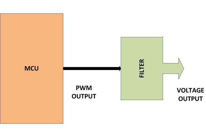
The following figure shows a microcontroller generating PWM wave which is then used to generate the corresponding analog voltage with the help of a filter circuit.

The filter could be any device which can generate the equivalent voltage of a PWM voltage. It normally consists of integrator, amplifiers, load drivers etc. They generate the voltage corresponding to the pulse width modulation in the wave and can fed that voltage to the load device.
In this particular project the filter circuit is actually an integrator made with a single capacitor. The filter simply integrates the duty cycle of each PWM cycles and hence averages out the voltage in a PWM wave as shown in the following figure;
The red colored lines shows the capacitors integration action on the PWM wave and the orange colored lines shows the average voltage that is available at the output of the integrator circuit corresponding to the PWM wave. In the above figure three different PWM waveforms are shown with PWM 1 has a duty cycle of 50% and it can generate an average voltage of almost half the voltage of the maximum voltage (logic 1 voltage) in the waveform. If the 5V logic is used to generate the PWM then this average voltage will be almost equal to 2.5V. The second waveform PWM 2 has a duty cycle of 10% only and it can generate an average voltage which is slightly greater than 0 only with the 5V logic. The third waveform PWM 3 has a duty cycle of 90% and it can generate an average voltage which is slightly less than the 5V logic.The above discuss things will happen only when the time period of the integrator is equal or slightly greater than the Period of the PWM. The integrator is a circuit which has a resistor and a capacitor in series connected across the input and the ground and the analog voltage is obtained across the capacitor as shown in the following figure;
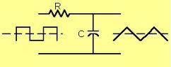
The product of the value of the resistance R and the value of capacitance C in the above circuit should be almost equal or slightly greater than the Period of the PWM wave.
RC >= PWM Period
From the calculations done for the Period of PWM wave, the value of the PWM Period is obtained as 2us. Hence for the proper generation of voltage according to the modulation of the pulses in the wave, the product RC should be equal or greater than 2us. Consider the 0.1uF capacitor is selected as C, and then the value of R required can be calculated as
RC >= 2us
R >= 2us / C
R >= 2 * 10^-6 / 0.1 * 10^-6
R >= 20 ohms.
Hence if the value for the C is taken as 0.1uF and the value of R is taken as 20 ohms, which will make an integrator circuit, required to generate the voltage equivalent of the PWM wave having a Period of 2us.
Note that the value of R is very small and this 20 ohm can be provided by the sum of the resistances of the built in resistance of the standard capacitor, the resistance of the microcontroller output pin, the resistance of the connecting wires etc. Hence there is practically no need to use a 20 ohm resistance, since a standard 0.1uf capacitor itself will do the job.
The circuit:
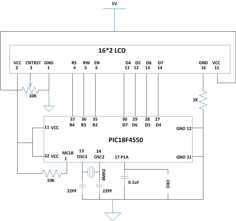
The circuit operates on well regulated 5V supply with a 4MHz external crystal oscillator which forms 48MHz CPU clock with the help of an internal PLL. The standard 0.1uF capacitor is used as the filter circuit (RC integrator) to generate the voltage equivalent of the PWM. The capacitor is connected across the PWM pin (PIN 17) of the microcontroller and the ground. The probe from the CRO is connected across the ground and the PWM pin of the microcontroller.
Tips for better results:
{C}{C}{C}{C}{C}{C}{C}{C}{C}{C}{C}{C}{C}· 1.Always use a well regulated power supply, since very small ripples in the power supply can induce noise in the PWM wave generated by the microcontroller and hence affects their voltage generation at the filter circuit.
{C}{C}{C}{C}{C}{C}{C}{C}{C}{C}{C}{C}{C}· 2.Use driver circuits as per the load requirement so as not to load or distort the PWM waveform
{C}{C}{C}{C}{C}{C}{C}{C}{C}{C}{C}{C}{C}· 3.{C}{C}{C}{C}{C}{C}{C}{C}{C}{C}{C}{C}{C}The period should not be less than which the load is not able to respond when using no filter circuits
{C}{C}{C}{C}{C}{C}{C}{C}{C}{C}{C}{C}{C}· 4.{C}{C}{C}{C}{C}{C}{C}{C}{C}{C}{C}{C}{C}The Duty-cycle should be select in such a way that it will generate the voltage in the range at which the load device can operate.
{C}{C}{C}{C}{C}{C}{C}{C}{C}{C}{C}{C}{C}· 5.{C}{C}{C}{C}{C}{C}{C}{C}{C}{C}{C}{C}{C}The filter circuit’s design should be precise so as to give maximum performance at the generated PWM Period and Duty-cycle.
{C}{C}{C}{C}{C}{C}{C}{C}{C}{C}{C}{C}{C}· 6.{C}{C}{C}{C}{C}{C}{C}{C}{C}{C}{C}{C}{C}Always operate the microcontroller at its maximum possible frequency so as to get maximum number of PWM cycles at any Sampling period, which will give a more stable voltage with the filter circuit or load.
{C}{C}{C}{C}{C}{C}{C}{C}{C}{C}{C}{C}{C}
{C}{C}{C}{C}{C}{C}{C}{C}{C}{C}{C}{C}{C}
{C}{C}{C}{C}{C}{C}{C}{C}{C}{C}{C}{C}{C}
Project Source Code
###
#include <p18f4550.h>#include <timers.h>//======================= chip config ===================//#pragma config PLLDIV = 1#pragma config CPUDIV = OSC1_PLL2#pragma config FOSC = HSPLL_HS#pragma config USBDIV = 1#pragma config IESO = OFF#pragma config PWRT = OFF#pragma config BOR = OFF#pragma config VREGEN = OFF#pragma config WDT = OFF#pragma config WDTPS = 32768#pragma config CCP2MX = ON#pragma config PBADEN = OFF#pragma config LPT1OSC = OFF#pragma config MCLRE = ON#pragma config STVREN = ON#pragma config LVP = OFF#pragma config ICPRT = OFF#pragma config XINST = OFF#pragma config DEBUG = OFF#pragma config WRTD = OFF//======================= chip config ===================////LCD Control pins#define rs PORTBbits.RB4#define rw PORTBbits.RB3#define en PORTBbits.RB2//LCD Data pins#define lcdport PORTD#define lcd_port_dir TRISDvoid lcd_clear ( void );void lcd_2nd_line ( void );void lcd_1st_line ( void );void lcd_ini ( void );void dis_cmd ( unsigned char cmd_value );void dis_data ( unsigned char data_value );void lcdcmd ( unsigned char cmdout );void lcddata ( unsigned char dataout );void delay_ms ( int delay );//=============== SINE WAVE LOOK UP TABLE ================//const unsigned char sine[50] = {52,57,62,66,70,74,77,80,82,84,85,86,86,86,85,83,81,78,75,72,69,65,61,56,52,48,44,39,35,31,28,25,22,19,17,15,14,14,14,15,16,18,20,23,26,30,34,38,43,48};//=============== SINE WAVE LOOK UP TABLE ================////============================ TIMER 0 ISR =================================//#pragma interrupt tmr0_interruptvoid tmr0_interrupt(void){static unsigned char i = 0;i ++;// method to write the sample values into the 10bit CCPR1 register //CCP1CON |= ( ( sine [ i ] ) << 5 ) & 0x03;CCPR1L = ( sine [ i ] ) >> 2;// method to write the sample values into the 10bit CCPR1 register //if ( i == 49 )i = 0;else;INTCONbits.TMR0IF=0; // clearing the timer0 overflow bit}//============================ TIMER 0 ISR =================================//void main ( void ){unsigned char data1 [] = "EngineersGarage";unsigned char data2 [] = " Sine Wave ";int i = 0;OSCCON = 0x0C;lcd_ini (); // LCD initializationdelay_ms ( 200 );//========================= start up display on LCD ================================//while ( data1 [i] != '�' ){dis_data ( data1 [i] );delay_ms ( 200 );i++;}i = 0;lcd_2nd_line ();while ( data2 [i] != '�' ){dis_data ( data2 [i] );delay_ms ( 200 );i++;}i = 0;/========================= start up display on LCD ================================////============================ PWM SETTINGS ====================================//TMR2 = 0x00; // setting TMR2 value as 0, start counting from 0PR2 = 22; // set the PR2 value, to get PWM period of 2usCCPR1L = 0x00; // setting initial value of CCPR1L as 0CCP1CON = 0x0C; // select single output with P1A, and mode select bits so as to getP1A, P1B, P1C and // P1D as active-highTRISC &= 0xFB; // setting the PWM pin as outputT2CON = 0x04; // both the pre-scalar and post-scalar bits are written for 1:1 with thetimer2 turned on.INTCONbits.T0IF = 0; // turning off the Timer0 interruptTMR0L = 0xFE; // setting the timer register to valueT0CON = 0xC0; // enable the timer, select the timer in 8bit, select CLKO,assign the pre-scale value 1:4INTCONbits.TMR0IF=0; // clearing the timer0 overflow bitINTCONbits.T0IE = 1; // enabling the timer0 interruptINTCONbits.GIE = 1; // enabling the global interrupts//============================ PWM SETTINGS ====================================//while ( 1 ){;}}//======================== LCD routines defenitions ========================//void delay_ms ( int delay ){int ms, i;for ( ms = 0; ms < delay; ms ++ )for ( i = 0; i < 70; i ++ );}void lcd_ini ( void ){TRISB &= 0xE3;lcd_port_dir &= 0x0F;dis_cmd ( 0x02 ); // to initialize LCD in 4-bit mode.dis_cmd ( 0x28 ); //to initialize LCD in 2 lines, 5X7 dots and 4bit mode.dis_cmd ( 0x0C );dis_cmd ( 0x06 );dis_cmd ( 0x80 );dis_cmd ( 0x01 );delay_ms ( 500 );}void dis_cmd ( unsigned char cmd_value ){unsigned char cmd_value1;cmd_value1 = cmd_value & 0xF0; //mask lower nibble because PA4-PA7 pins are used.lcdcmd ( cmd_value1 ); // send to LCDcmd_value1 = ( ( cmd_value << 4 ) & 0xF0 ); //shift 4-bit and masklcdcmd ( cmd_value1 ); // send to LCD}void dis_data ( unsigned char data_value ){unsigned char data_value1;data_value1 = data_value & 0xF0;lcddata ( data_value1 );data_value1 = ( ( data_value << 4 ) & 0xF0 );lcddata ( data_value1 );}void lcdcmd ( unsigned char cmdout ){lcdport &= 0x0F;lcdport |= cmdout;rs = 0;rw = 0;en = 1;delay_ms ( 50 );en = 0;delay_ms ( 50 );}void lcddata ( unsigned char dataout ){lcdport &= 0x0F;lcdport |= dataout;rs = 1;rw = 0;en = 1;delay_ms ( 50 );en = 0;delay_ms ( 50 );}void lcd_clear(void){dis_cmd(0x01);delay_ms(10);}void lcd_2nd_line(void){dis_cmd(0xC0);delay_ms(1);}void lcd_1st_line(void){dis_cmd(0x80);delay_ms(1);}//======================== LCD routines defenitions ========================//
###
Circuit Diagrams
Project Components
Project Video
Filed Under: PIC Microcontroller.
Filed Under: PIC Microcontroller.

Questions related to this article?
👉Ask and discuss on Electro-Tech-Online.com and EDAboard.com forums.
Tell Us What You Think!!
You must be logged in to post a comment.