In the previous article, we learned what a low-power system is so now we’ll talk about the key factors using which we can make power-efficient embedded system design.
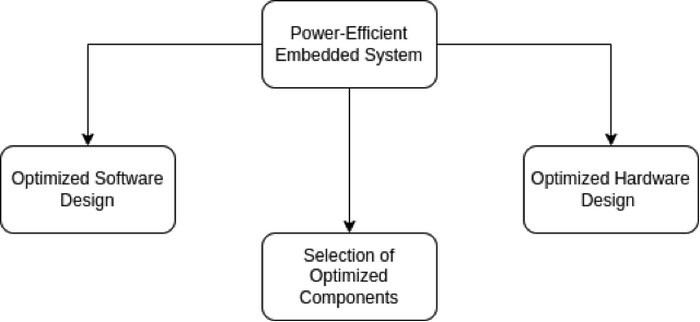
The power-efficient embedded system is comprised of hardware and software design along with proper components selection. Optimization is achieved by efficient implementation in different stages using different techniques. The available techniques are given below.
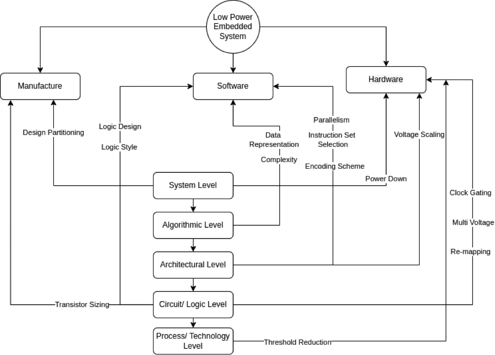
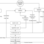
Higher levels of power reduction techniques include system, algorithmic and architectural levels, as well as lower levels of power reduction techniques including circuit and process level. The higher levels provide larger amounts of power reduction for chip designs giving designers a greater degree of freedom to implement low-power (up to 70 percent reduction) design techniques. Hence, the power-optimization process is the most effective method for higher levels of abstraction. Let’s learn more about these levels in detail.
System level
System level generally includes the techniques which can be implemented during customized manufacturing of IC’s or at Hardware Design. The system level techniques are the following:
- Hardware/Software Partitioning. The mapping of a system level into specific hardware(FPGA, ASIC etc.) and software(Code running on CPU, MCU etc) components based upon their requirement.
- Task characterization. This step helps in developing a low-energy implementation strategy to characterize tasks according to processing frequency, processing time, and hardware algorithm alternatives. This is important because the strategies for implementation will depend heavily on these characteristics.
Algorithmic level
The most effective design decisions derive from choosing and optimizing algorithms at the highest levels. This technique is used at this level where the number of operations that require larger power is reduced. This approach also reduces the number of switching activities which leads to a decrease in switched capacitance of the overall system, thus reducing the dynamic power consumption of the system. For example, arithmetic or register units of a microprocessor will perform only when such logic commands are invoked, so we can disable the logic commands which are not in use during a particular clock cycle.
Architectural level
Different techniques at the architectural level are applied to minimize dynamic power dissipation in arithmetic circuits, especially in digital multipliers. Some of the architectural level techniques are:
- Parallelism. Concurrent execution of several programs or several blocks of a program is known as parallel processing. Parallelism can be done by multi-core architecture. By replicating the same core several times the incoming inputs are applied to different cores in sequence.
- Voltage Scaling. In this technique, the overall operating voltage of the device is kept low for the entire board as power consumption is directly proportional to the operating voltage. For example, if all the chips can work on 2.7 V, then you would keep a margin of 1 V and set that voltage for the board. When the processor supply voltage is reduced, the speed of the system slows. To supplement this, software techniques like pipelining can be used to maintain the throughput of the system explained in software techniques.
- Pipelining. The process of accumulating instruction from the processor through a pipeline. It allows storing and executing instructions in an orderly process. Pipelining does not reduce power by itself but, instead, reduces the critical path delay by inserting registers between combinational logic. Pipelining also reduces the instructions per clock cycle (IPC), due to high branch misprediction penalties and other hazards, and thus can reduce energy efficiency. The timing slack from pipelining can be used for voltage scaling and gate downsizing to achieve significant power savings.
Logic and Circuit level
Logic and circuit level generally include techniques that can be implemented during customized manufacturing of ICs or at the hardware and software design. Some of the logic and circuit level techniques are:
- Transistor sizing. The process of reducing or increasing the channel width of the transistor at the time of manufacturing. The smaller your transistors, the more transistors can fit on a chip, and the faster and more efficient the processor can be. For example, if the size of the transistor is 25 μm then the drive current will be just 0.9mA and if the size is 100 μmk then the drive current will be 20mA.
- Clock gating. A technique used in many synchronous circuits for reducing dynamic power dissipation by removing the clock signal when the circuit is not in use. This can be achieved by adding Enable Circuit which will pass the use of the clock when Enable is high and vice versa. These circuits can be a gate, tristate buffer, latch, etc.
Process / Technology level
Threshold Voltage. The reduction of the voltage swing (swing is the difference between the maximum output voltage and minimum output voltage), and reduction of the effective load capacitance (sum of load capacitance and parasitic capacitance), reducing power dissipation. Also, reducing VDD in non-critical paths will help in reducing power consumption.
Component Selection
- Use of more static than dynamic circuits as the static power loss is very less in a dynamic logic circuit.
- Selecting the right input voltage for the embedded board is important, Whether we are using a battery or an adapter for the power supply. For example, if all the circuitry on the board is powered by 5 V or 3.3 V then using a 5 V – 6 V power input is better than using a 12/24V DC input or battery input.
- Boost circuits are generally inefficient. If you have a choice to use buck conversion, use buck instead of boost.
- The quiescent current of a power supply is the amount of current which is consumed at zero or no load. Always use a low quiescent current power supply, as it has very high efficiency at the current range your circuit will be consuming.
Circuit Design Level The designer has several options while designing a low-power system including the following:
- Choose the low-power components in the design. For example, while selecting an IC, consider an IC with low power (active / Idle) consumption and a low operating voltage rating.
- Optimize the size of the PCB such that you can minimize the power consumption of the electronic circuits.
- Placement of the component in such a way that signal track length can be minimized and signal propagation time is as fast as possible to minimize any power loss.
Low power embedded system design benefits
- A low Power system produces a lesser amount of heat which will be good for the environment.
- The embedded system’s working cycle is improved due to less power dissipation.
- The low Power system also helps in reducing the production cost as these systems will be simpler and cost-effective.
Conclusion
The successful design and evaluation of an embedded system requires proper power management. In this article, we have reviewed most of the levels of design where power reduction techniques can be incorporated.
You may also like:
Filed Under: Power, Tech Articles, Tutorials




Questions related to this article?
👉Ask and discuss on Electro-Tech-Online.com and EDAboard.com forums.
Tell Us What You Think!!
You must be logged in to post a comment.