[[wysiwyg_imageupload:1961:]]This Project is contributed by Mr. Siddharth Jain from Faridabad.
Presently, the United States is the most technologically advanced country in the area of telecommunications with about; 126 million phone lines, 7.5 million cellular phone users, 5 thousand AM radio broadcast stations, 5 thousand FM radio stations, 1 thousand television broadcast stations, 9 thousand cable television systems, 530 million radios, 193 million television sets, 24 ocean cables, and scores of satellite facilities!
This is truly an “Information Age” and sometimes, you need to look at where we’ve been in order to see the future more clearly!!
Information
—“A message received and understood” — Princeton
—“Information is a term with many meanings depending on context, but is as a rule closely related to such concepts as meaning, knowledge, instruction, communication, representation, and mental stimulus ” — Wikipedia
— “any communication or representation of knowledge such as facts, data, or opinions in any medium or form, including textual, numerical, graphic, cartographic, narrative, or audiovisual forms (OMB Circular A-130). ” — Gils.net
— “Facts, concepts, or instructions; any sort of knowledge or supposition which can be communicated.” — cedar.web.cern
— “Is organized data that has been arranged for better comprehension or understanding.
What is one person’s information can become another person’s data.” — earthlink.net
Information transfer
A coordinated sequence of user and telecommunications system actions that cause information present at a source user to become present at a destination user.
Broadcast
A term to describe communication where a piece of information is sent or transmitted from one point to all other points. There is just one sender, but the information is simultaneously sent to all connected receivers. In networking, a distinction is made between broadcasting and multicasting. Broadcasting sends a message to everyone on the network whereas multicasting sends a message to a select list of recipients.
One of the most common examples is broadcast through a cellular network service. This serves multiple end users at different locations in a simulcast fashion.
Practically every cellular system has some kind of broadcast mechanism. This can be used directly for distributing information to multiple mobiles, commonly, for example in a mobile telephony system, the most important use of broadcast information is to set up channels for one to one communication between the mobile Trans-receiver and the base station. This is called paging. The details of the process of paging vary somewhat from network to network, but normally we know a limited number of cells where the phone is located (this group of cells is called a location area in the GSM system or Routing Area in UMTS). Paging takes place by sending the broadcast message on all of those cells.
Today, interaction with digital displays is a deskbound or device-dependent experience. However, developments in display and information sharing technologies may enable a new form of interaction with digital media: ‘ubiquitous computing’. In ubiquitous computing, the physical location of data and processing power is not apparent to the user. Rather, information is made available to the user in a transparent and contextually relevant manner. A single display device restricts the repertoire of interactions between the user and digital media, so ubiquitous computing requires displays wherever the user might need one – in appliances, tabletops public transport, walls, etc.
This project aims at integrating the expansiveness of a wireless cellular network and the ease of information transfer through the SMS with the coverage of public display boards. It is thereby a modest effort to realize the complete potential of public display boards in instantaneous information broadcast in swift response to events of interests.
PROJECT DESCRIPTION
Recently, the health care sensors are playing a vital role in hospitals. The patient monitoring systems is one of the major improvements because of its advanced technology. A wireless patient monitoring system to measure heartbeat and body temperature of the patient by using embedded technology is developed.
So we are here, just connecting the temperature sensor and heartbeat sensor so that simultaneously we can monitor the patient’s condition and hence ruling out the use of the thermometer and other devices to check the condition of the patient.
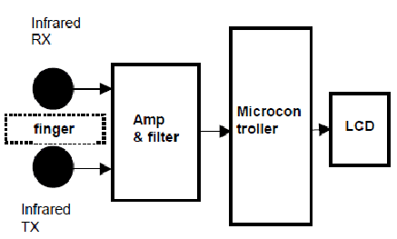
This project describes the design of a simple, low-cost microcontroller based heart rate & body temperature measuring device with LCD output. Heart rate of the subject is measured from the index finger using IRD (Infra Red Device sensors and the rate is then averaged and displayed on a text based LCD).
The device alarms when the heart beat & the body temperature exceed the provided threshold value. This threshold value is defined by the programmer at the time of programming the microcontroller 89C8051. The threshold value given for the project is as 20 to 120 pulses per minute for heart beat indication & 18°C to 38°C for temperature.
This information i.e. the Heart Rate & the Body Temperature is then transmitted wirelessly to the doctor which in not in the vicinity of the patient through GSM technique. The sensors measure the information and transmit it through GSM Modem on the same frequency as on which cell phones work.
IDEA of the TRANSMISSION BETWEEN TRANSMITTER AND RECEIVER
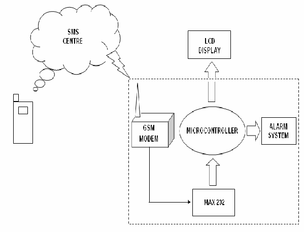
[BASIC IDEA OF GSM BASED TOOL KIT SHOWING TRANSMITTER AND RECEIVER PART AND THE INFORMATION AS THE SMS ]
IDEA of the PROJECT THROUGH BLOCK DIAGRAM
COMPONENTS
The Major Componets used in Our Project are:
2. MAX 232
3. LCD DISPLAY
4. ADC CONVERTER
5. LM35 ( TEMPERATURE SENSOR)
6. SIM 300 GSM MODEM
7. CRYSTAL 11.0592 MHz
8. BUZZER
9. CAPACITORS
10. RESISTORS
11. CONNECTING WIRES
12. POWER SUPPLY
GSM MODEM
A GSM modem is a wireless modem that works with a GSM wireless network. A wireless modem behaves like a dial-up modem. The main difference between them is that a dial-up modem sends and receives data through a fixed telephone line while a wireless modem sends and receives data through radio waves. Like a GSM mobile phone, a GSM modem requires a SIM card from a wireless carrier in order to operate.
Matrix Simado GDT11 is a Fixed Cellular Terminal (FCT) for data applications.
It is a compact and portable terminal that can satisfy various data communication needs over GSM. It can be connected to a computer with the help of a standard RS232C serial port. Simado GDT11 offers features like Short Message Services (SMS), Data Services (sending and receiving data files), Fax Services and Web Browsing. Remote login and data file transfer are also supported. It is the perfect equipment for factory plants, resorts, dams and construction sites where wired connectivity is not available or not practicable. The Simado GDT11 is easy to set up. It finds its applications in IT companies, Banks and Financial Institutions, Logistic Companies, Service Providers, Remote Project Sites, Professionals, and such other business establishments.
Computers use AT commands to control modems. Both GSM modems and dial-up
modems support a common set of standard AT commands. GSM modem can be used just like a dial-up modem. In addition to the standard AT commands, GSM modems support an extended set of AT commands. These extended AT commands are defined in the GSM standards. With the extended AT commands, various things can be done:-
- Reading, writing and deleting SMS messages.
- Sending SMS messages.
- Monitoring the signal strength.
- Monitoring the charging status and charge level of the battery.
- Reading, writing and searching phone book entries.
The number of SMS messages that can be processed by a GSM modem per minute is very low — only about six to ten SMS messages per minute.
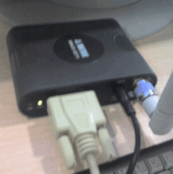
Simado GDT11
Accessing GSM MODEM using Microsoft HyperTerminal
Microsoft HyperTerminal is a small program that comes with Microsoft Windows. We use it to send AT commands to the GSM modem. It can be found at
Start -> Programs -> Accessories -> Communications -> HyperTerminal.
Before programming our SMS application, it is required to check if the GSM modem and SIM card are working properly first. The MS HyperTerminal is a handy tool when it comes to testing the GSM device. It is a good idea to test the GSM devices beforehand.
When a problem occurs, sometimes it is difficult to tell what causes the problem. The cause can be the program, the GSM device or the SIM card. If GSM device and SIM card with MS HyperTerminal and they operate properly, then it is very likely that the problem is caused by the program or other hard wares.
For Linux users, Mincom can be used instead of HyperTerminal.
Testing of GSM MODEM
To use MS HyperTerminal to send AT commands to the GSM modem, the following procedure is followed:
- We put a valid SIM card into the GSM modem. We can obtain a SIM card by subscribing to the GSM service of a wireless network operator.
- Since in our case the modem drivers were pre installed, we need not to install any such drivers.
- Then we start up MS HyperTerminal by selecting Start -> Programs -> Accessories -> Communications -> HyperTerminal.
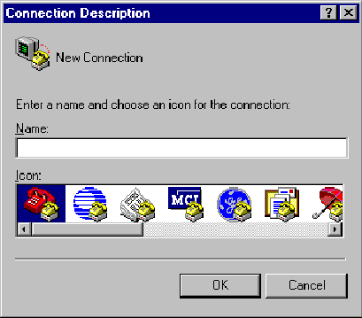
- In the Connection Description dialog box (as shown in the screenshot given below), we enter any name and choose an icon we like for the connection. Then we click the OK button.
- In the Connect To dialog box, choose the COM port that your mobile phone or GSM modem is connecting to in the Connect using combo box. For example, choose COM1 if your mobile phone or GSM modem is connecting to the COM1 port. Then click the OK button.(Sometimes there will have more than one COM port in the Connect using combo box. To know which COM port is used by your mobile phone or GSM modem, follow the procedure below.
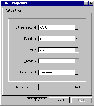
- The Properties dialog box comes out. Enter the correct port settings for your mobile phone or GSM modem. Then click the OK button.
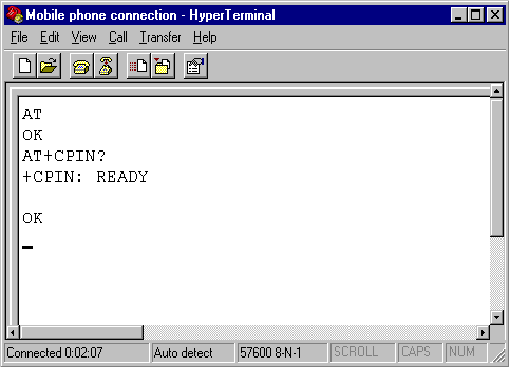
- Type “AT” in the main window. A response “OK” should be returned from the mobile phone or GSM modem. Type “AT+CPIN?” in the main window. The AT command “AT+CPIN?” is used to query whether the mobile phone or GSM modem is waiting for a PIN (personal identification number, i.e. password). If the response is “+CPIN: READY”, it means the SIM card does not require a PIN and it is ready for use. If your SIM card requires a PIN, you need to set the PIN with the AT command “AT+CPIN=<PIN>”.
If you get the responses above, your mobile phone or GSM modem is working properly.
LCD DISPLAY
Read the following article for details
MICROCONTROLLER – Atmel AT89C51
Read the following articles for details
OSCILLATOR CHARACTERISTICS
XTAL1 and XTAL2 are the input and output, respectively, of an inverting amplifier that can be configured for use as an on-chip oscillator, as shown in Figure 11-1. Either a quartz crystal or ceramic resonator may be used. To drive the device from an external clock source, XTAL2 should be left unconnected while XTAL1 is driven, as shown in Figure 11-2. There are no requirements on the duty cycle of the external clock signal, since the input to the internal clocking circuitry is through a divide-by-two flip-flop, but minimum and maximum voltage high and low time specifications must be observed.
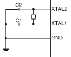
Oscillator Connections
Note: C1, C2 = 30 pF ± 10 pF for Crystals.
= 40 pF ± 10 pF for Ceramic Resonators.
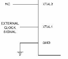
External Clock Drive Configuration
MICROCONTROLLER – MODEM INTERFACING
DTE and DCE
The terms DTE and DCE are very common in the data communications market. DTE is short for Data Terminal Equipment and DCE stands for Data Communications Equipment. As the full DTE name indicates this is a piece of device that ends a communication line, whereas the DCE provides a path for communication.
For example, the PC is a Data Terminal (DTE). The two modems (yours and that one of your provider) are DCEs, they make the communication between you and your provider possible.
RS-232
In telecommunications, RS-232 is a standard for serial binary data signals connecting between a DTE (Data terminal equipment) and a DCE (Data Circuit-terminating Equipment). It is commonly used in computer serial ports. In RS-232, data is sent as a time-series of bits. Both synchronous and asynchronous transmissions are supported by the standard. In addition to the data circuits, the standard defines a number of control circuits used to manage the connection between the DTE and DCE. Each data or control circuit only operates in one direction that is, signaling from a DTE to the attached DCE or the reverse. Since transmit data and receive data are separate circuits, the interface can operate in a full duplex manner, supporting concurrent data flow in both directions. The standard does not define character framing within the data stream, or character encoding.
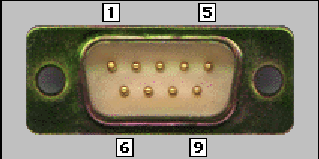
Female 9 pin plug
|
Functions
|
Signals
|
PIN
|
DTE
|
DCE
|
|
Data
|
TxD
|
3
|
Output
|
Input
|
|
RxD
|
2
|
Input
|
Output
|
|
|
Handshake
|
RTS
|
7
|
Output
|
Input
|
|
CTS
|
8
|
Input
|
Output
|
|
|
DSR
|
6
|
Input
|
Output
|
|
|
DCD
|
1
|
Input
|
Output
|
|
|
STR
|
4
|
Output
|
Input
|
|
|
Common
|
Com
|
5
|
—
|
—
|
|
Other
|
RI
|
9
|
Output
|
Input
|
RS-232 Signals
RS-232 Signals
- Transmitted Data (TxD)
Data sent from DTE to DCE.
- Received Data (RxD)
Data sent from DCE to DTE.
- Request To Send (RTS)
Asserted (set to 0) by DTE to prepare DCE to receive data. This may require action on the part of the DCE, e.g. transmitting a carrier or reversing the direction of a half-duplex line.
- Clear To Send (CTS)
Asserted by DCE to acknowledge RTS and allow DTE to transmit.
- Data Terminal Ready (DTR)
Asserted by DTE to indicate that it is ready to be connected. If the DCE is a modem, it should go “off hook” when it receives this signal. If this signal is de-asserted, the modem should respond by immediately hanging up.
- Data Set Ready (DSR)
Asserted by DCE to indicate an active connection. If DCE is not a modem (e.g. a null-modem cable or other equipment), this signal should be permanently asserted (set to 0), possibly by a jumper to another signal.
- Carrier Detect (CD)
Asserted by DCE when a connection has been established with remote equipment.
- Ring Indicator (RI)
Asserted by DCE when it detects a ring signal from the telephone line.
RTS/CTS Handshaking
The standard RS-232 use of the RTS and CTS lines is asymmetrical. The DTE asserts RTS to indicate a desire to transmit and the DCE asserts CTS in response to grant permission. This allows for half-duplex modems that disable their transmitters when not required and must transmit a synchronization preamble to the receiver when they are re-enabled. There is no way for the DTE to indicate that it is unable to accept data from the DCE. A non-standard symmetrical alternative is widely used: CTS indicates permission from the DCE for the DTE to transmit, and RTS indicates permission from the DTE for the DCE to transmit. The “request to transmit” is implicit and continuous. The standard defines RTS/CTS as the signaling protocol for flow control for data transmitted from DTE to DCE. The standard has no provision for flow control in the other direction. In practice, most hardware seems to have repurposed the RTS signal for this function. A minimal “3-wire” RS-232 connection consisting only of transmits data, receives data and
Ground, and is commonly used when the full facilities of RS-232 are not required. When only flow control is required, the RTS and CTS lines are added in a 5-wire version. In our case it was imperative that we connected the RTS line of the microcontroller (DTE) to ground to enable receipt of bit streams from the modem.
Specifying Baud Rate, Parity & Stop bits
Serial communication using RS-232 requires that you specify four parameters: the baud rate of the transmission, the number of data bits encoding a character, the sense of the optional parity bit, and the number of stop bits. Each transmitted character is packaged in a character frame that consists of a single start bit followed by the data bits, the optional parity bit, and the stop bit or bits. A typical character frame encoding the letter “m” is shown here.
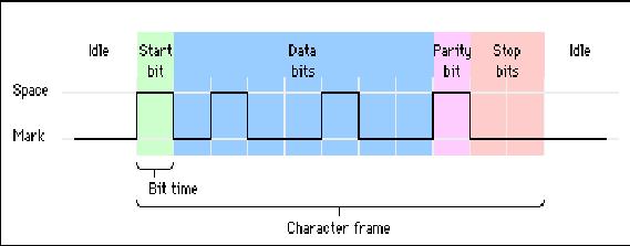
Character Frame Encoding ‘m’
We specified the parameters as baud rate – 2400 bps, 8 data bits, no parity, and 1 stop bit (2400-8-N-1). This was set in pre-operational phase while setting up the modem through the hyper terminal, as per the serial transmission standards in 8051 microcontroller.
MICROCONTROLLER – LCD INTERFACING
See the article Microcontroller interfacing with LCD
MAX 232
See details of MAX 232
ANALOG / DIGITAL CONVERTER
See ADC0804
TEMPERATURE SENSOR (LM 35)
See LM35
OPERATIONAL AMPLIFIER (LM 324)
The LM124 series consists of four independent, high gain, internally frequency compensated operational amplifiers which were designed specifically to operate from a single power supply over a wide range of voltages. Operation from split power supplies is also possible and the low power supply current drain is independent of the magnitude of the power supply voltage.
Application areas include transducer amplifiers, DC gain blocks and all the conventional op amp circuits which now can be more easily implemented in single power supply systems. For example, the LM124 series can be directly operated off of the standard +5V power supply voltage which is used in digital systems and will easily provide the required interface electronics without requiring the additional ±15V power supplies.
Pin Configuration: 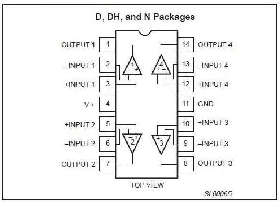
UNIQUE FEATURES:
In the linear mode, the input common-mode voltage range includes ground and the output voltage can also swing to ground, even though operated from only a single power supply voltage. The unity gain crossover frequency and the input bias current are temperature-compensated.
FEATURES:
- Internally frequency-compensated for unity gain.
- Large DC voltage gain: 100 dB.
- Wide bandwidth (unity gain): 1 MHz (temperature-compensated)
- Wide power supply range Single supply: 3 VDC to 30 VDC or dual supplies: ±1.5 VDC to ±15 VDC.
- Very low supply current drain: essentially independent of supply voltage (1 mW/op amp at +5 VDC).
- Low input biasing current: 45 nADC (temperature-compensated)
- Low input offset voltage: 2 mVDC and offset current: 5 nADC.
- Differential input voltage range equal to the power supply voltage.
- Large output voltage: 0VDC to VCC–1.5 VDC swing.
QUAD VOLTAGE COMPARATOR (LM339)
The LM139 series consists of four independent precision voltage comparators, with an offset voltage specification as low as 2.0 mV max for each comparator, which were designed specifically to operate from a single power supply over a wide range of voltages. Operation from split power supplies is also possible and the low power supply current drain is independent of the magnitude of the power supply voltage. These comparators also have a unique characteristic in that the input common-mode voltage range includes ground, even though they are operated from a single power supply voltage. The LM139 series was designed to directly interface with TTL and CMOS. When operated from both plus and minus power supplies, the LM139 series will directly interface with MOS logic where their low power drain is a distinct advantage over standard comparators.
Pin Configuration:
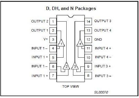
FEATURES:
- Wide single supply voltage ranges 2.0 VDC to 32 VDC or dual supplies ±1.0 VDC to ±16 VDC.
- Very low supply current drain (0.8 mA) independent of supply voltage (1.0 mW/comparator at 5.0 VDC)
- Low input biasing current 25 nA.
- Low input offset current ±5 nA and offset voltage.
- Input common-mode voltage range includes ground.
- Differential input voltage range equal to the power supply voltage.
- Low output 250 mV at 4 mA saturation voltage.
- Output voltage compatible with TTL, DTL, ECL, MOS and CMOS logic systems.
Applications:
- High precision comparators.
- Reduced VOS drift over temperature.
- Eliminates need for dual supplies.
- Allows sensing near GND.
- Compatible with all forms of logic.
- Power drain suitable for battery operation.
DUAL OPERATIONAL AMPLIFIER (Op amp)
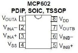
The MCP602 dual operational amplifier (op amp) has a gain bandwidth product of 2.8 MHz with low typical operating current of 230 and an offset voltage that is less than 2 mV. The MCP602 uses Microchip’s advanced CMOS technology, which provides low bias current, high-speed operation, high open-loop gain and rail-to-rail output swing. The MCP602 operates with a single supply voltage that can be as low as 2.7V, while drawing 230 ?A (typ.) of quiescent current per amplifier. In addition, the common mode input voltage range goes 0.3V below ground, making these amplifiers ideal for single-supply operation. These devices are appropriate for low-power, battery operated circuits due to the low quiescent current, for A/D convert driver amplifiers because of their wide bandwidth or for anti-aliasing filters by virtue of their low input bias current.
This amplifier is ideal for industrial process control, low-power battery-operated devices, portable equipment, data acquisition equipment, test equipment and low-end audio applications.
Temperature Range (°C) = -40°C to +125°C
And, Power Supply Range = 2.7V to 5.5V
Pin Configuration:
Features:
- Single-Supply: 2.7V to 5.5V
- Rail-to-Rail Output
- Input Range Includes Ground
- Gain Bandwidth Product: 2.8 MHz (typ.)
- Unity-Gain Stable
- Low Quiescent Current: 230 ?A/amplifier (typ.)
- Chip Select (CS): MCP603 only
- Temperature Ranges:
- Industrial: -40°C to +85°C
- Extended: -40°C to +125°C
- Available in Single, Dual and Quad
Typical Applications:
- Portable Equipment
- A/D Converter Driver
- Photo Diode Pre-amp
- Analog Filters
- Data Acquisition
- Notebooks and PDAs
- Sensor Interface
SCHMITT TRIGGER
Schmitt trigger is a generic name of threshold circuits with positive feedback having a loop gain > 1. The circuit is named “trigger” because the output retains its value until the input changes sufficiently to trigger a change: in the non-inverting configuration, when the input is higher than a certain chosen threshold, the output is high; when the input is below a different (lower) chosen threshold, the output is low; when the input is between the two, the output retains its value. This dual threshold action is called hysteresis and implies that the Schmitt trigger possesses memory and can act as a bistable circuit (latch). There is a close relation between the two kinds of circuits that actually are the same: a Schmitt trigger can be converted into a latch and vice versa, a latch can be converted into a Schmitt trigger. 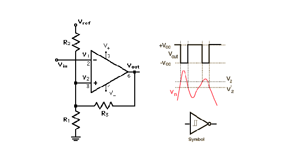
Schmitt trigger devices are typically used in open loop configurations for noise immunity and closed loop negative feedback configurations to implement bistable regulators, triangle/square wave generators, etc.
The Schmitt trigger is a comparator application which switches the output negative when the input passes upward through a positive reference voltage. It then uses negative feedback to prevent switching back to the other state until the input passes through a lower threshold voltage, thus stabilizing the switching against rapid triggering by noise as it passes the trigger point.
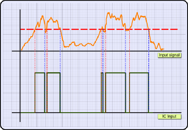
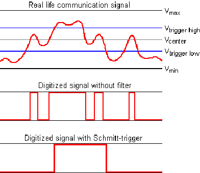 Schmitt Trigger Voltage Levels
The first graph shows the actual input signal. There is quite some noise on the line, and if the center voltage is used to determine if the input is in the on, or off state, there can be four high periods detected in the signal as shown in the second graph. If we however use two trigger levels with hysteresis, it is possible to reduce the number of detected logical highs to only one. This is what the Schmitt trigger does in the last graph.
The simplest Schmitt Trigger circuit is implemented with a comparator with a positive feedback. Look at the following circuit:
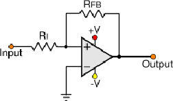
When the non-inverting input (+) is higher than the inverting input (-), the comparator output switches to the POSITIVE voltage supply. On the contrary, the non-inverting input (+) is lower than the inverting input (-), the output switches to the NEGATIVE voltage supply.
The inverting input (-) is grounded, so someone would expect that the turn-on and off point would be the ground (0). The function of the ST comes from the feedback resistor RFB. When for example the output of the comparator is to the POSITIVE voltage supply, then the non-inverting input has through the RFB this voltage! The same happens when the output is to the NEGATIVE power supply.
The voltage needed to switch the output of the comparator must be above or below zero (ground), according to the POSITIVE and NEGATIVE power supply and according to the resistors RI and RFB. More specific, the formula to calculate the threshold voltage is: 
So, if the output is to the POSITIVE voltage, the required negative voltage that must be applied to Vin is:
VINPUT <= – VTHRESHOLD
If the output is to the NEGATIVE voltage, the required positive voltage that must be applied to Vin is:
VINPUT >= VTHRESHOLD
The above circuit is non-inverting Schmitt Trigger. It can be easily converted into an inverting Schmitt Trigger as follows:
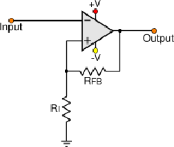
The same formula is used to calculate the threshold level. But the output of this circuit is inverted in comparison to the previous one. When the input voltage is above the High Threshold Level, the output goes LOW.
These are the most basic Schmitt Trigger. The threshold voltage is an equal offset from the center of the POSITIVE and NEGATIVE power supply (usually this is 0). Thus, we can call it “Symmetrical Schmitt Trigger”.
Use of Schmitt Trigger:
From the analog signal which also contains the noise signal we get the digital signal.
Programming Code
See Attachments for the program
Advantages of Proposed Method
• The staying of specialist is eliminated.
• It is a multipurpose so that overall conditions are easily measured.
• Easy to operate.
• Compare with compact sensor it gives better performance.
• Modern technologies have developed that promotes comfortable and better life which is disease free.
• PREVENTION IS BETTER THAN CURE
APPLICATIONS
The project is used to transfer the information from the transmitter side to the receiver side wirelessly. The project is an advance application of GSM based DISPLAY TOOLKIT.
In our project we are basically focussing on the situation where the where the patient(s) and the doctor are at the distant location and it is quite necessary to give the details about the patient(s) heartbeat and the tempearture to the doctor. In this type of situation where the information becomes the indespensable part of the life this project emerges out as best to acknowledge the doctor witth he correct and the fast information.
Besides this if made certain changes in the project, it can also be used as way of acknowledging the students of the institutes with the fastest mode of information regarding certain Notices. Again it is the application of GSM BASED DISPLAY TOOLKIT.
Looking into current trend of information transfer in the campus, it is seen that important notice take time to be displayed in the notice boards. This latency is not expected in most of the cases and must be avoided.
Also the electronics displays which are currently used are programmable displays which need to be reprogrammed each time a new notice comes. The process of reprogramming includes burning the microcontroller again and again. This makes it inefficient for immediate information transfer, and thus the display board looses its importance.
CONCLUSION
This Project which demonstrates an automated patient monitoring system has its own merits and demerits which are discussed below:
Merits:
The wireless alert system using WAP notifies physicians of critical results on their Display (Cellular Phones can also be used as a display).
- With online recording of medical parameters, the workload of the case providers and the nursing staff is reduced.
- The clinical information database contains all data regarding the patients in electronic form.
- The patient call switches help emergency situations to be handled quickly.
Future enhancements can be easily implemented with the PLC controller.
De-Merits:
- The heart beat sensor is highly temperature dependent and the dynamic characteristics change with different levels of ambient light and temperature level.
- The dual operational amplifier needs a high CMRR and additional narrowband filters are necessary to attenuate effects of the noise interference.
- Network Congestion and Noise interference involved, delays the transmission and reception of the signal, hence delayed observations are obtained.
FUTURE ENHANCEMENTS
The entire medical data acquisition could be made wireless and wearable. Such a package would contain the circuiting for inputs from ECG sensors, EEG sensors, pressure measurement and pulse rate transducers. This wearable module can transmit the data continuously over a fiber optic link or through an internet digital radio. The received data can be stored in separate memory and be processed by a microcontroller. This enhancement will enable monitoring of patients to be more flexible and strain-free.
In addition to above the following enhancement can also be made:
• A graphical LCD can be used to display a graph of the change of heart rate over time.
• Sound can be added to the device so that a sound is output each time a pulse is received.
• The maximum and minimum heart rates over a period of time can be displayed.
• Serial output can be attached to the device so that the heart rates can be sent to a PC for further online or offline analysis.
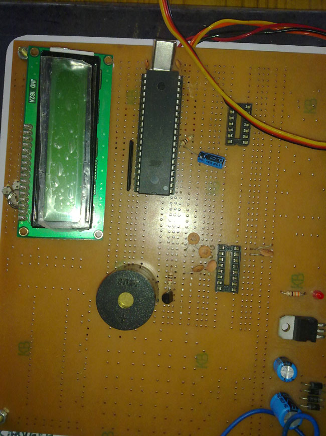
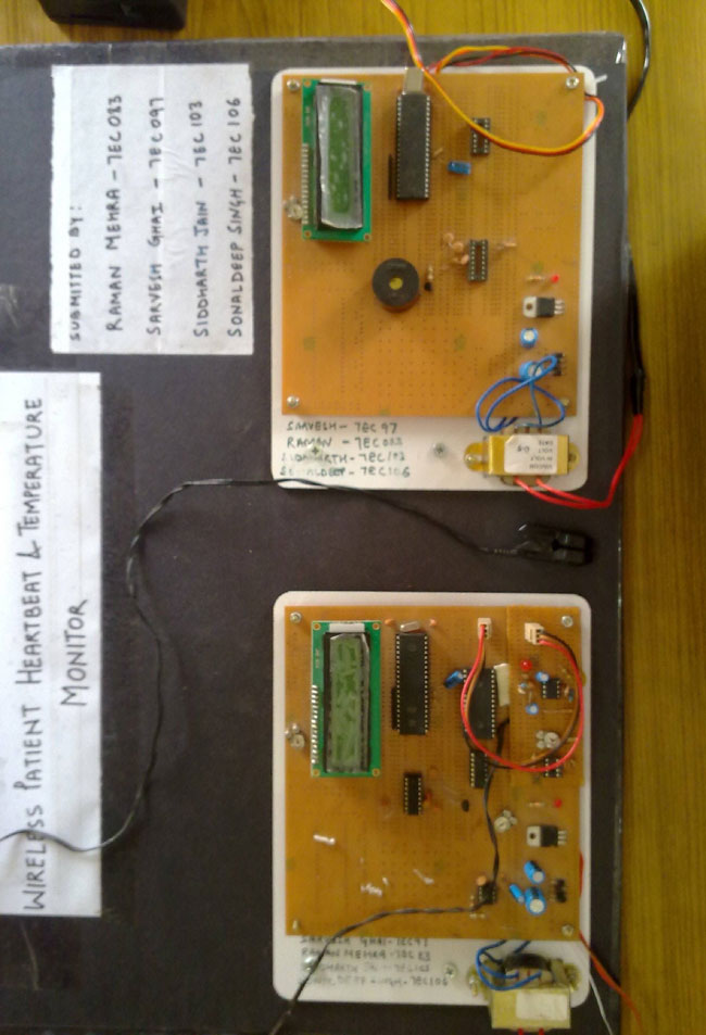
Project Snapshots
Transmitter 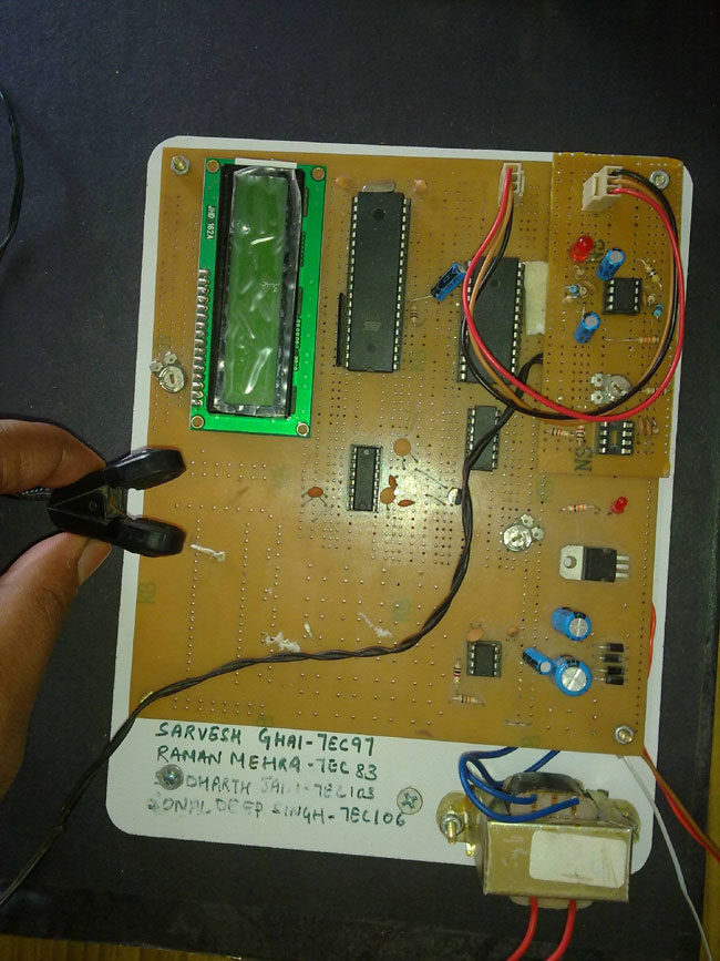 Receiver
Receiver
Project Source Code
Circuit Diagrams
| WIRELESS-PATIENT-HEARTBEAT-AND-TEMPERATURE-MONITORING-SYSTEM21 | 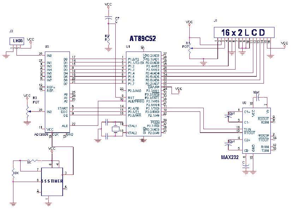 |
| WIRELESS-PATIENT-HEARTBEAT-AND-TEMPERATURE-MONITORING-SYSTEM23 | 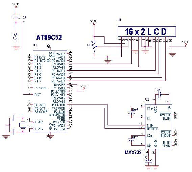 |
Project Datasheet
Filed Under: Electronic Projects

Questions related to this article?
👉Ask and discuss on EDAboard.com and Electro-Tech-Online.com forums.
Tell Us What You Think!!
You must be logged in to post a comment.