This tutorial explains how to write the content in the microcontroller’s flash memory. The source microcontroller writes some values in the memory of the target microcontroller. The values that have been written can be checked by reading the buffer of the target microcontroller using a programmer. The values are nothing but the machine language instruction written in the hex file generated by a compiler.
The reader should know the basics of sending and receiving the single byte in programming mode. Refer to 8051 Programmer basics before reading this project.
There are two modes of writing values in a microcontroller. The table below shows the instruction corresponding to memory write operation. In case of write operation the memory needs to be erased first.


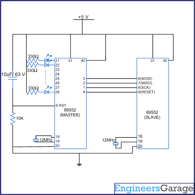
Fig. 1: Circuit Diagram of 8051 Programmer
4. Byte Mode
In this mode the values are written one by one. You need to send the address of the memory location in every instruction whose value is to be written. The first byte of the instruction signifies memory write operation (byte mode). The second and third byte tells the address of the memory location. Some bits of the second byte are don’t care. This is because the maximum size of flash memory for this family is 8K and in order to address the last memory location a maximum of 13 bits is required. The fourth byte contains the data which is to be written in the specified memory location of the target microcontroller.
2. Page mode
The memory of the microcontroller is arranged in form of pages. Every page contains 256 bytes arranged in 16 rows and 16 columns. In this mode a chunk of 256 bytes is written in one write instruction. The second byte of the instruction sends the address of the page where the data needs to be written. The 256 bytes of data is sent consecutively from the third byte of the instruction. No instruction is accepted till 265 data bytes are written.
Circuit and Algorithm
Circuit Diagram

Fig. 2: Circuit Diagram of 8051 Programmer
Algorithm
Algorithm for Byte mode:
1. Power on the circuit.
2. Send the instruction for programming enable.
3. Check the 4th byte on MISO pin. If we receive 0x69 this means chip is enabled.
4. If the serial programming mode is enabled then send the chip erase instruction.
5. Send the instruction corresponding to memory write (byte mode). It should have the address and data to be written.
6. Keep repeating step 5 till all the bytes are written in the target microcontroller.
Algorithm for Page write mode:
1. Power on the circuit.
2. Send the instruction for programming enable.
3. Check the 4th byte on MISO pin. If we receive 0x69 this means chip is enabled.
4. If the serial programming mode is enabled then send the chip erase instruction.
5. Send first byte to enable page write mode followed by the address of the page.
6. After the address bytes the 256 data bytes of data is sent on the MOSI pin.
7. Keep repeating step 6 till all the pages you want to write are written.
Code
Code
The following code is used to write the bytes in the memory of the controller which are verified using a programmer. This code writes four bytes using the byte mode.
#include <REG51.h>
#include<intrins.h>
#define port P1

sbit sck=port^0;
sbit res=port^3;
sbit miso=port^1;
sbit mosi=port^2;

bit bit1;
unsigned int i,bitno=0;
unsigned char a,b,c,d;
void delay(unsigned int msec)   // Function for delay
{
	int i,j;
	for(i=0;i<msec;i++)
		for(j=0;j<1275;j++);
}

void sendbit()
{
	mosi=bit1;
	delay(1);
	_nop_();
	sck=1;
	delay(1);
	_nop_();
	sck=0;
}

void sendbyte(unsigned char m)
{
	for(bitno=0;bitno<8;bitno++)
	{
		bit1=m/128;
		m=m<<1;
		sendbit();
	}
}

void main()
{
	i=0;
	sck=0;
	res=1;
	delay(500);

//=======Program enable===========

	a=0xac;
	b=0x53;
	c=0x00;
	d=0x11;
	sendbyte(a);
	sendbyte(b);
	sendbyte(c);
	sendbyte(d);

//==========Erase==================

	a=0xac;
	b=0x82;
	c=0x12;
	d=0x13;
	sendbyte(a);
	sendbyte(b);
	sendbyte(c);
	sendbyte(d);

//===========write=================

	sendbyte(0x40);
	sendbyte(0x00);
	sendbyte(0x00);
	sendbyte(0xEE);

	sendbyte(0x40);
	sendbyte(0x00);
	sendbyte(0x01);
	sendbyte(0x12);

	sendbyte(0x40);
	sendbyte(0x00);
	sendbyte(0x02);
	sendbyte(0x5C);

	sendbyte(0x40);
	sendbyte(0x00);
	sendbyte(0x03);
	sendbyte(0xAB);

	res=1;
	while(1);
}
Filed Under: Tutorials


Questions related to this article?
👉Ask and discuss on EDAboard.com and Electro-Tech-Online.com forums.
Tell Us What You Think!!
You must be logged in to post a comment.