In A guide to bipolar junction transistors, the definition and types of transistors and their applications are covered. In What to look for in a BJT transistor datasheet, transistor specifications are discussed, including what’s required before using or choosing a transistor in a circuit. In this article, we’ll explain what transistor configurations are and why they’re used.
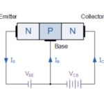
A transistor is a current-controlled device. How it works: In a transistor, the current flows from an emitter to a collector, which increases proportionally to a small current at the base of the transistor. The biasing voltage at its base controls the conduction of the current.
The output of a transistor (meaning the current from the collector) can be in three regions:
1. The cut-off region: Occurs when the emitter- and collector-base junctions are reverse-biased. The transistor is fully OFF in this region, so the collector current is zero.
2. The saturation region: Occurs when the emitter- and collector-base junctions are forward-biased. The transistor is fully ON in this region, and the collector current suddenly rises from zero to a saturation current level.
3. The active region: Occurs when the emitter-base junction is forward-biased and the collector-base junction is reversed-biased. In this region, the transistor operates as an amplifier and the collector current is equivalent to the emitter current.
The base current controls the emitter-collector current. The collector current is amplified by a gain constant for the given operating point (biasing condition) compared to the base current.
A transistor can switch digital signals by operating in the cut-off and saturation regions or amplify analog signals by operating in the active region. As transistor is a three-terminal device, meaning it can connect in three different configurations in a circuit, where one terminal remains common between the input and the output.
These three configurations are:
- Common-base
- Common-emitter
- Common-collector
All three configurations yield different output characteristics, as discussed next.
Common-base configuration
In common-base configuration, the transistor’s base terminal remains common between the input and the output. The base terminal is connected to the ground or to a fixed reference voltage. The input signal is applied to the transistor’s emitter, and the load is connected to its collector.
The circuit diagram below shows the common-base configuration for an NPN transistor.
![]()
The common-base configuration for the PNP transistor is shown below.
![]()
The common-base configuration offers an unexpected high-voltage gain but attenuates the current. In a transistor, the emitter current (IE) is always equal to the sum of the base current (IB) and the collector current (IC). In the common-base configuration, the emitter current is divided into the base current and the collector current. So, the collector current is always slightly less than the emitter current.
As the emitter current is the input and collector current is output, the current gain in a common-base configuration is always equal to or less than 1. The current gain in common-base configuration is represented by a quantity called alpha (α), where α is the ratio of collector current to emitter current.
αdc = IC/IE (for DC mode)
α = ∆IC/∆IE @ VCB = constant (for AC mode)
The current gain “α” typically remains between 0.9 and 0.99. It’s dependent on the transistor’s physical construction rather than its configuration in the circuit.
The current gain “α” typically remains between 0.9 and 0.99. It is dependent on the transistor’s physical construction rather than its configuration in the circuit.
In this configuration, the input and output voltage are in phase and remain nearly the same amplitude. An almost equal change follows a small change in the base-emitter voltage (input voltage) in the base-collector voltage (output voltage). The input characteristics of the common-base configuration are represented by variations in the emitter current in terms of the base-emitter voltage for the constant base-collector voltages. The input characteristics are similar to the forward-bias characteristics of a diode.

As seen in the above chart, changes in the collector-base voltage have a negligible effect on the emitter current. The emitter current follows diode characteristics with respect to the base-emitter voltage. The emitter current rises exponentially to a constant value after the base-emitter voltage crosse 0.7 V, regardless of the collector-base voltage.
The transistor becomes fully ON when the base-emitter voltage crosses 0.7 V, regardless of the voltage at the base-collector junction.
The output characteristics of the common-base configuration are represented by variations of the collector current with respect to the base-collector voltage for specific emitter current levels.
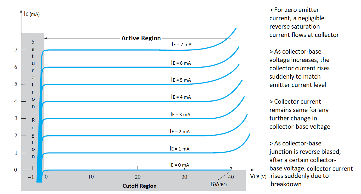
When the emitter current is zero, a negligible reverse saturation current flows through the collector due to minority carriers. As the collector-base voltage increases, the collector current rapidly matches the emitter current level. The collector current remains nearly equal to the emitter current for any further increment in the collector-base voltage.
When the collector-base junction is reverse-biased for the transistor to operate in the active region, increasing the collector-base voltage further can reach a breakdown voltage level. At this point, the collector-base junction experiences an avalanche effect, causing a sharp rise in the collector current.
At the input stage, the emitter-base junction is forward-biased, allowing the transistor to turn ON or remain in the active region. The emitter current increases exponentially with the emitter-base voltage, resulting in low input impedance for the transistor.
At the output stage, the collector-base junction is reverse-biased, causing the collector current to remain constant despite increases in collector-base voltage until the junction reaches its breakdown voltage. This gives the transistor a high output impedance. Since the voltage amplitude is nearly the same at both the input and output, and the output current is attenuated, the collector-base configuration yields minimal power gain.
Due to low power gain, common-base configuration is not typically used for amplification. However, it is still used in audio pre-amplifier and RF amplifiers because of its excellent frequency response. The common-base configuration is also used for impedance matching as the input stage has low impedance and the output stage of this transistor configuration offers high impedance. This configuration may also be used to attenuate current signals.
Common-emitter configuration
In the common-emitter configuration, the emitter terminal of the transistor remains common between the input and the output. The emitter terminal is connected to the ground or a fixed reference voltage. The input signal is applied at the base of the transistor, and the load is connected to the transistor collector.
This is the most common configuration for transistor amplifiers. The circuit diagram below shows the common-emitter configuration for an NPN transistor.
![]()
The common-emitter configuration for an PNP transistor is below.
![]()
The common-emitter configuration offers the highest power and current gains of the three transistor configurations. In this configuration, the base current is the input, and the collector current is the output. The base current is typically in the microampere range, while the collector current is in the milliampere range.
Due to the physical construction of a transistor, a small change in the base current results in a large change in the emitter-to-collector current. The current gain in common emitter configuration is given by a quantity called beta (β), where β is the ratio of collector current to base current.
β = IC/IB (for DC mode)
β = ∆IC/∆IB @ VCE = constant (for AC mode)
The value of β typically ranges from 20 to 200, depending on the physical construction of the transistor. It’s independent of the configuration in the circuit. This means the collector current is at least 20 times greater than for any value of the base current. If β is 100 for a transistor, the collector current is 100 times more than the base current.
The output voltage has a phase shift of 180 degrees with respect to the input voltage. This is because the base current flows through a forward-biased emitter-base junction while the collector current flows through a reverse-biased base-collector junction. The emitter-collector voltage is greater in amplitude than the base-emitter voltage. As the internal resistance of the transistor is fixed and the current gain results in a much higher current flowing through the collector, the voltage is amplified due to the voltage-current relationship (V = IR).
This configuration’s input characteristics are represented by variations in the base current with respect to base-emitter voltage for constant collector-emitter voltages. The input characteristics are similar to the forward-bias characteristics of a diode except that the base current is inversely affected by the collector-emitter voltage.
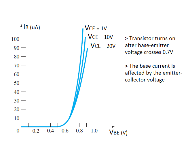
As indicated in the above chart, the base current rises exponentially after the base-emitter voltage exceeds 0.7 V, causing the transistor to turn ON. The magnitude of the base current is affected by the collector-emitter voltage of the output stage.
The output characteristics of the common-emitter configuration are represented by variations in the collector current in regard to the emitter-collector voltage for specific base current levels.
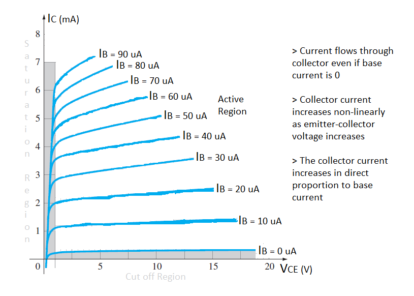
In a common-emitter configuration, the collector current is not zero even when the base current is zero. As the emitter-collector voltage increases, the collector current also increases, even with a zero base current. This current depends on the transistor’s current gain, α, and is described by the following equation.
Beyond a certain fixed collector-emitter voltage, the transistor remains fully ON. The collector current increases non-linearly with the emitter-collector voltage and is amplified proportionally to the base current. When the collector-base junction is reverse-biased for the transistor to turn ON and operate in the active region, further increases in the emitter-collector voltage can lead to an avalanche effect and transistor breakdown.
In the common-emitter configuration, the emitter-base junction is forward-biased, resulting in medium input impedance. The emitter-collector output shows high output impedance due to the transistor’s internal resistance between the emitter and collector and the reverse-bias of the collector-base junction.
The common-emitter configuration offers the highest power and current gain among all three transistor configurations, as both current and voltage are amplified with minimal opposition from the transistor’s internal resistance.
This makes it the most suitable configuration for using a transistor as an amplifier. It’s commonly employed in audio power amplifiers, signal amplifiers for sensors, and for driving high-power loads such as speakers and actuators. Most amplifier circuits use bipolar transistors in the common-emitter configuration.
Common-collector configuration
In the common-collector configuration, the collector terminal of the transistor remains common between the input and the output. The collector is connected to the ground or a fixed reference voltage. The input signal is applied at the transistor’s base of the load is connected to its emitter. The circuit diagram below shows the common-collector configuration for an NPN transistor.
![]()
The common-collector configuration for an PNP transistor is shown below.
![]()
In a transistor, the emitter current is the sum of the collector and base currents. In the common-collector configuration, the output current (emitter current) is significantly higher than the input current (base current). The relationship between the emitter current and the base current is given by the following equation.
IE = IB (1 + β)
As the value of β for a general-purpose transistor ranges from 20 to 200, the current gain of the common-collector configuration (per the above equation) is greater than 20.
In the common-collector configuration, the output voltage is in phase with and equal in amplitude to the input voltage, which is why it is also known as an emitter-follower or voltage follower. Both the input and output voltages are in phase because they both pass through the same reverse-biased collector-base junction. The voltage gain is unity, as the collector resistance is much higher than the emitter resistance due to the transistor’s construction.
This results in nearly the same voltage drop across the emitter-collector stage as across the collector-base junction.
The input characteristics of the common-collector configuration are represented by the variations in the base current with respect to the base-collector voltage for constant collector-emitter voltages. These input characteristics are similar to the reverse-bias characteristics of a diode, with the horizontal and vertical scales inverted. The base current serves as the input current for both the common-collector and common-emitter configurations.
However, in the common-collector configuration, the sign of the collector-emitter voltage is reversed compared to the common-emitter configuration. In the common-emitter configuration, the input stage involves a forward-biased base-emitter junction, while in the common-collector configuration, it is a reverse-biased base-collector junction.
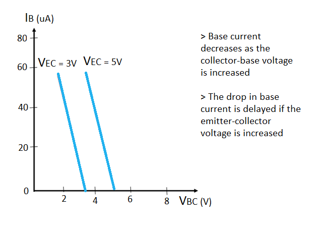
Noticeably, the base current decreases with increasing collector-base voltage, primarily due to the reverse biasing of the collector-base junction. This decrease in base current is further delayed when the emitter-collector voltage is raised. The output characteristics of the common-collector configuration depict the variation of the emitter current concerning the emitter-collector voltage at specific base current levels.
Given that “α” typically ranges from 0.9 to 0.99, the collector current in the common-emitter configuration can be approximated by the emitter current in the common-collector configuration. Consequently, the output characteristics of the common-collector configuration align closely with those of the common-emitter configuration.

In the common-collector configuration, the input stage has a high impedance due to the reverse-biased collector-emitter junction. The output stage has a very low impedance due to the forward-biased emitter-base junction. As the current is amplified but the voltage amplitude remains the same for the input and output, the power gain in the common collector configuration is medium.
The common-collector configuration is used for building current amplifiers where a small change in base current results in a large emitter current. The configuration is also used as a voltage follower to drive high-current low-impedance loads. It’s also used as an impedance buffer to interface high-impedance circuits with low-impedance circuits without affecting the signal strength (the voltage gain is unity for the common-collector configuration).
Comparison of the transistor configurations
The following table summarizes the key differences between the common-base, common-emitter, and common-collector configurations.

You may also like:


Filed Under: Tech Articles
Log in to leave a comment:
Lost your password?
Don't have an account? Register here