
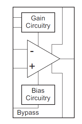
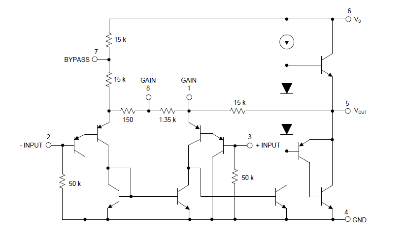
Fig. 2: Block Diagram of Audio Power Amplifier
Circuit Connections –
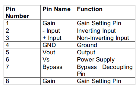
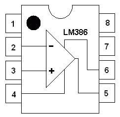
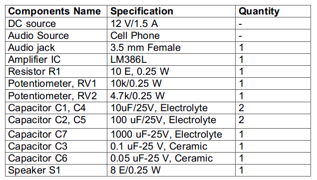
This IC is basically an operational amplifier whose voltage gain can be adjusted by using a proper RC circuit between its gain setting pins. If the gain setting pins are left open, the voltage gain of the amplifier is internally set to 20 (26 dB). For adjusting the gain between the desired range of 20 (26 dB) and 200 (46 dB), a variable resistor (Shown as RV2 in the circuit diagram) of 4.7 Kilo ohms and a capacitor (Shown as C1 in the circuit diagram) of 10 uF are connected between the pins 1 and 8 of the IC. For controlling the output volume level, a variable resistor (Shown as RV1 in the circuit diagram) is connected at the input of the non-inverting pin. This variable resistor actually changes the amplitude (input voltage level) of the input signal as amplitude defines the loudness of the audio signal.
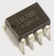
Fig. 8: Typical Image of LM386 Audio Power Amplifier IC
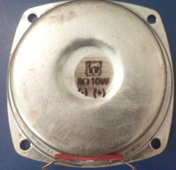
While assembling this circuit following precautions must be taken care of –
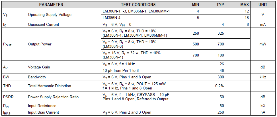
So, with a supply voltage set to 12V and a load of 8 ohms at the output, the power output of the amplifier can be approximately 1 Watt.


You may also like:
Project Video
Filed Under: Audio, Tutorials
Filed Under: Audio, Tutorials






Questions related to this article?
👉Ask and discuss on EDAboard.com and Electro-Tech-Online.com forums.
Tell Us What You Think!!
You must be logged in to post a comment.