Components Required

How the circuit works –

Fig. 2: Prototype of Power Bank designed on a breadboard
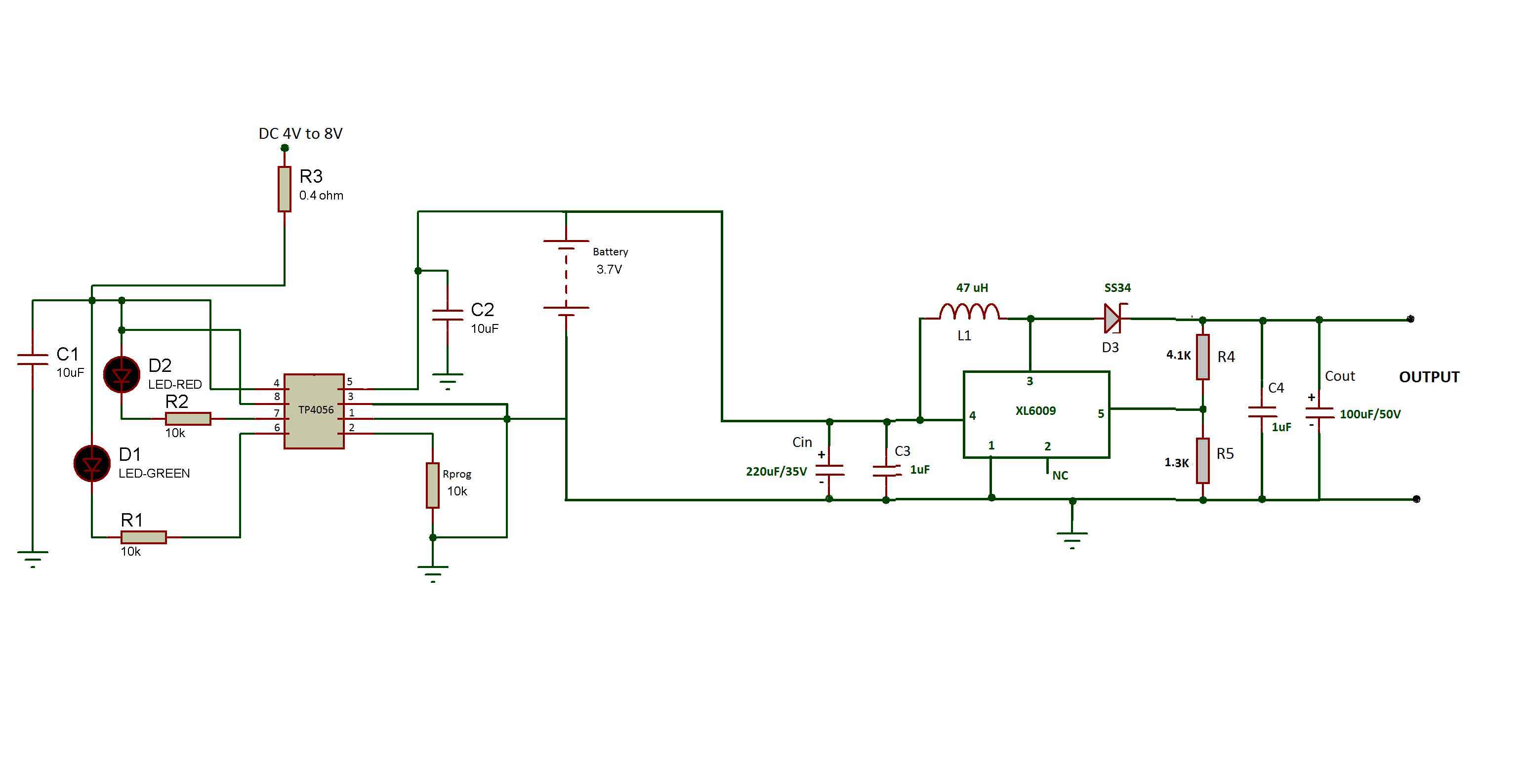
The circuit of the power bank has two building blocks – 1) Battery recharge circuit and 2) Output amplifier circuit. If the output voltage required would have been 3.7 V or 4 V only, the amplifier circuit would not have been required. But, the required output voltage is 5V, that is why amplifier circuit at the output of the device is a must. As per the circuit sections, the device also operates in two stages – 1) Charging of the battery and 2) Taking the output from the battery through amplifier circuit.
1) Charging of the Li-ion battery with TP4056 charger

The IC needs minimum 4V to 8V voltage for its operation. It can provide maximum 1000mA charging current to the battery and a fixed 4.2 V at the output. The circuit as given in the datasheet of the IC is used to design the charger.
Fig. 4: Circuit Diagram of TP4056 IC based Power Bank Battery Charger
For deciding the value of charging current of the battery a Rprog resistor has to be connected at the PROG pin as described the function of the PROG pin in the datasheet.
For 1000mA charging current Rprog can be calculated as follows –
Ibat = ( VPROG/RPROG )*1200 (VPROG = 1V)
Rprog = (Vprog/Ibat)*1200
Rprog = (1/1)*1200
Rprog = 1.2k
The battery should be connected as per polarity indicated on the IC because the TP4056 IC does not have any reverse polarity protection circuit.
o Battery Charging Indicators
For visual indication of charge termination and charging state of the battery, LEDs can be connected to pin 6 and pin 7 of the IC. When the input supply is provided to the circuit then the Red LED at pin 7 lights up which will indicate the charging state of the battery. When the battery voltage will reach to 4.2V then the battery will draw less current. The charging current when drops down to 1/10th of the programmed current (1000mA) then charging will be terminated. The Green LED at pin 6 will light up and give a visual indication that the battery is fully charged (as terminal voltage has reached 4.2V).
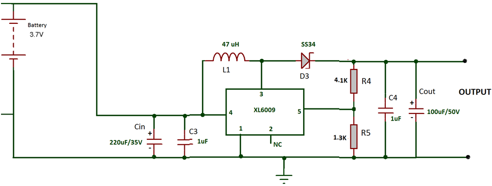
2) Drawing output from the battery through Voltage amplifier and regulator circuit –

The circuit specified in the datasheet of the IC for typical boost converter application is used in this project.
Note: You can find the XL6009 Boost Converter Circuit under the “Circuit Diagram 2” tab.

Internally the XL6009 has N-channel power MOSFET with fixed frequency of the oscillator (as in below fig 4). This MOSFET acts as a switching transistor and oscillator which generates a square wave of around 400kHz (as per the datasheet). During the positive half-cycle of the square wave, the inductor stores some energy and generates a magnetic field so the left terminal of the inductor is a positive voltage and right one is at negative. Therefore the anode of the diode is at lower potential and acts like an open circuit.
Vout = 1.25*(1+(R4/R5))
As R4 =4.1k and R5= 1.3k
Vout = 1.25*(1+(R4/R5))
By putting R4 and R5 values in above equation
Testing –

You may also like:


Circuit Diagrams
Filed Under: Electronic Projects
Log in to leave a comment:
Lost your password?
Don't have an account? Register here