In the previous tutorial, basics of sequential logic circuits were discussed. It was mentioned that sequential circuits can be of two types – synchronous and asynchronous. The sequential circuits are different from combinational circuits in the way that they have memory elements for feedback of previous input states. The asynchronous circuits use latches as the memory elements. The latches cannot be used as memory elements in synchronous circuits as the synchronous circuits require transition sensitive devices to operate against clock signals. So, for synchronous circuits, flip flops are used as memory elements.
The flip flops themselves are built on latches. For making a flip flop, the operation of the basic latch is modified by providing an additional control input that determines when the state of the circuit is to be changed. So, basically, the latch with the additional control input is called the flip flop. The additional control input is either the clock or enable input.
The Flip Flops are categorized into different types depending on how their inputs and clock pulses cause transition between two states. There are four basic types of flip flops as follow –
1) S – R Flip Flop
2) J – K Flip Flop
3) D Flip Flop
4) T Flip Flop
SR Flip Flop –
The SR flip flop is simply the SR latch with enable input. The SR latch with Enable input has been described in the previous tutorial. This is the simplest flip flop. The SR latch is built by two cross-coupled NOR gates. The Enable input is added by connecting two additional NAND gates to the basic circuit of the SR latch. So, SR flip Flop has two output Q and Q’ which are complement of each other and three inputs – Set (S), Reset (R) and Enable (En). The clock pulse is applied to the enable input. The flip flop changes state only when it is set HIGH (in case Enable input is active high) or when it is set LOW (in case Enable input is active low). The enable input can be made active low by connecting an inverter gate before it. The SR Flip Flop has the following logic gate diagram –
Fig. 1: Logic Gate Diagram of SR Flip Flop
It can be represented by the following block diagram –

Fig. 2: Block Diagram of SR Flip Flop
It operates according to the following function table –

Fig. 3: Truth Table of SR Flip Flop
It can be observed from the function table that when S = 0 and R = 0 the output of NAND gates 3 and 4 are forced to become 1. Hence R’ and S’ both will be equal to 1. Since S’ and R’ are the input of the basic S-R latch using NAND gates, there will be no change in the state of outputs. When S = 0 and R = 1, since S = 0, output of NAND-3 i.e. R’ = 1 and E = 1 the output of NAND-4 i.e. S’ = 0. Hence Qn+1 = 0 and Qn+1 bar = 1. This is called reset condition. When S = and R = 0. output of NAND-3 i.e. R’ = 0 and output of NAND-4 i.e. S’ = 1. Hence output of S-R NAND latch is Qn+1 = 1 and Qn+1 bar = 0. This is called set condition. As S = 1, R = 1 and E = 1, the output of both NAND gates 3 and 4 are 0 i.e. S’ = R’ = 0. Hence the forbidden condition will occur in the basic NAND latch.
D Flip Flop –
The D Flip Flop is built from the D latch. It is designed to avoid forbidden condition in the SR flip flop. The D (Delay) flip flop has only one input called the delay input, the two outputs Q and Ǭ and the Enable input to receive clock pulses. A D Flip Flop is constructed by coupling inputs to NAND gates in an SR Flip Flop. While coupling the NAND gates in first level of the logic gate implementation of the D Flip Flop, the Data input is directly connected to Set (S) input of the SR latch while it is connected through an inverter to the Reset (R) input of the SR latch. This way, when Data (D) is 0, Set is 0 and Reset is 1 while when D is 1, Set is 1 and Reset is 0. A D flip flop has the following logic gate diagram –
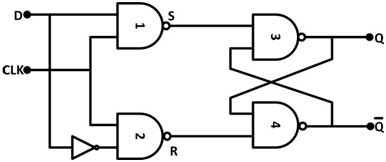
Fig. 4: Logic Gate Diagram of D Flip Flop
A D flip flop can be represented by the following logic gate diagram –
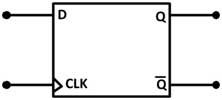
Fig. 5: Block Diagram of D Flip Flop
The D Flip Flop operates according to the following function table –
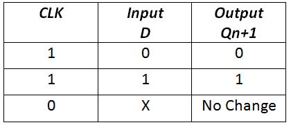
Fig. 6: Truth Table of D Flip Flop
From the function table, it can be observed that when the CLK input is LOW, the D input has no effect, since the set and the reset inputs of the NAND flip – flop are kept HIGH. When the CLK goes HIGH, the Q output will take on the value of the D input. If CLK = 1 and D = 1, the NAND gate -1 output goes 0 which is the S bar input of basic NAND based S-R flip flop and NAND gate-2 goes 1 which is the R bar input of the basic NAND based S-R flip flop. Therefore S bar = 0 and R bar = 1, the flip flop output will be 1, i.e. it follows D input. For CLK = 1 and D = 0, the flip flop output will be 0. If D changes while CLK is HIGH, Q will follow and change quickly.
From the function table it is clear that the next state of the flip flop at any time (Qn +1) follows the value of the input D when the clock pulse is applied. As transfer of data from the input to the output is delayed, it is known as delay (D) flip flop. The D flip-flop is used as the delay device or as a latch to store 1 bit of binary information.
Master Slave JK Flip Flop –
The Master Slave JK Flip Flop is designed to avoid forbidden condition in the SR flip flop along with eliminating the timing problem for response to the high and low levels of the clock pulse. The Master Slave JK Flip-Flop is constructed by cascading two S-R Flip-flop with feedback from the output of second to the input of first. This way, Master flip flop is a positive level triggered. But due to the presence of the inverter in the clock line, the slave will respond to the negative level. Hence when the clock signal is 1 (positive level), the master is active and the slave is inactive. Whereas when clock is 0 (low level), the slave is active and master is inactive.
The JK flip flop has three inputs J, K and Enable input while two outputs Q and Q’. The JK Flip Flop has the following logic gate diagram –
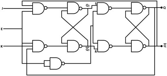
Fig. 7: Logic Gate Diagram of Master Slave JK Flip Flop
It operates according to the following function table –

Fig. 8: Truth Table of Master Slave JK Flip Flop
From the function table it can be observed that there are four possible outputs of JK flip flops as mentioned below –
Case 1 – J = K = 0 (No change): When clock signal is 0, the slave becomes active and master inactive. But, since the S and R inputs have not changed, the slave outputs will also remain unchanged. Therefore outputs will not change if both J and K are 0.
Case 2 – J = 0 and K = 1 (Reset): When Clock signal is 1, Master is active while slave is inactive. Therefore, outputs of the master become Q1 = 0 and Q1 bar = 1. That means S becomes 0 and R becomes 1. When Clock signal is 0, the Slave is active while master is inactive. Therefore, outputs of the slave become Q = 0 and Q bar = 1. Again when clock signal is 1, the Master is active and slave is inactive. Therefore even with the changed outputs (Q = 0 and Q bar = 1) fed back to the master, its output will be Q1 = 0 and Q1 bar = 1. That means, S becomes 0 and R becomes 1. Hence with clock signal being 0 and slave becoming active, the outputs of slave will remain Q = 0 and Q bar = 1. Thus, there is a stable output from the Master and Slave.
Case 3 – J = 1 and K = 0 (Set): When Clock signal is 1, Master is active and slave is inactive. Therefore, outputs of the master become Q1 = 1 and Q1 bar = 0. That means, S is set to 1 and R set to 0. When Clock signal is 0, the Slave is active and master is inactive. Therefore outputs of the slave become Q = 1 and Q bar = 0. Again when clock signal is 1, then it can be seen that the outputs of the slave are stabilized to Q = 1 and Q bar = 0.
Case 4 – J = K = 1 (Toggle): When Clock signal is 1, the Master is active and slave is inactive. The outputs of master will toggle. So S and R will also be inverted. When Clock signal is 0, the Slave is active and master is inactive. The outputs of slave will toggle. These changed outputs are returned back to the master inputs. But, when clock signal is 0, the master is still inactive. So it does not respond to these changed outputs. This avoids the multiple toggling which leads to the race around condition. The master slave flip flop is useful in avoiding the race around condition of SR flip flop.
T Flip Flop –
The T flip flop or Toggle Flip Flop changes its output on each clock edge. It is another basic flip flop which has only a single data (T) input, a clock input and two outputs Q and Ǭ. The T – type flip-flop is constructed from JK flip flop by connecting its J and K inputs together. The T stands for the ability of the flip flop to toggle or complements its state. A T Flip Flop is represented by the following block diagram –
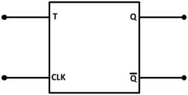
Fig. 9: Block Diagram of T Flip Flop
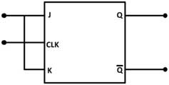
Fig. 10: Logic Gate Diagram of T Flip Flop
The T Flip Flop operates according to the following function table –

Fig. 11: Truth Table of T Flip Flop
From the function table, it can be seen that when the T input is in 0 state (i.e. J=K=0) prior to clock pulse, the Q output will not change with clocking. When the T input is set to 1 level (i.e. J = K = 1) prior to clocking, the output will be in the Ǭ state after clocking. In other words, if the T input is logical 1 and the device is clocked, the output will change state regardless of what output was prior to clocking. So, when T = 0, then Qn+1 = Qn , i.e. the next state is the same as the present state and no change occurs. When T = 1, then Qn+1 = Ǭn , i.e. the state of the flip-flop is complemented. This is called toggling so the flip flop got its name T flip-flop.
Flip-Flops are essential part of any synchronous circuit. They can store a single bit at a time. The groups of flip flops are used to store data in practical synchronous circuits. In the next tutorial, learn about registers.
You may also like:
Filed Under: Digital Electronics, Tutorials




Questions related to this article?
👉Ask and discuss on EDAboard.com and Electro-Tech-Online.com forums.
Tell Us What You Think!!
You must be logged in to post a comment.