In this era of battery-operated devices, a DC-DC converter is needed to meet the divergent power requirements of the electronic circuitry. A battery is a type of DC Supply whose output voltage varies with its use. This means it cannot maintain a constant voltage at the output due to its discharging characteristics. For this reason, regulators are used to regulate the supply at constant voltage. To regulate the supply and shift the supply to a constant voltage, step-up or step-down converters are used.
A step-down converter, also known as a buck converter, is used to shift down the voltage supply, whereas a step-up converter, also known as a boost converter, is used to shift up the voltage supply.
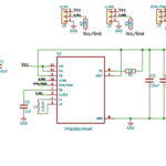
In this experiment, we will design a step-up converter that will take supply from a Li-Ion battery and provide an output constant of 12 V DC. For this purpose, we will use MT3608 IC; we will test the converter for an output current of up to 250m A.

Figure 1. Pinout of MT3608 IC
About MT3608
The MT3608 is a step-up DC-DC Converter intended for small, low-power applications. It is manufactured by Aerosemi and has the following major features:
- High switching frequency (1.2 MHz). This allows the use of a low-cost inductor and capacitor.
- Wide input voltage range (2 V to 24 V). This makes it suitable for a 3.7 V Li-Ion battery as input.
- Adjustable output voltage up to 28 V
- Up to 97 % efficiency
- Internal current limit at 4A
MT3608 Pinout
| Pin | Description |
| 1 | Power switch output. It is the drain of the internal MOSFET |
| 2 | Ground |
| 3 | Feedback Input to regulate the output voltage |
| 4 | Enable pin to make converter ON/OFF. High on this pin makes converter turns ON, low makes converter turns OFF |
| 5 | Input voltage supply pin |
| 6 | No connection |
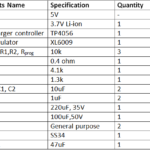
Component Selection
The IC needs external components to act as a DC-DC converter. The following biasing components are needed:
- Inductor
- Diode
- Capacitor
- Resistor

Figure 2. The circuit connection of Li-on to 12V DC convertor with MT3608
Inductor (L1)
The inductor is the energy storage element in a DC-DC converter. It stores energy when the MOSFET is switched ON and delivers the stored energy to output when MOSFET gets switched OFF. The energy stored in the inductor makes it act as a power source, and it adds to the input power which shifts the output voltage higher than the input.
As per the datasheet, an inductor of 4.7uH to 22uH is suitable for the application. The current rating of the inductor must be greater than the maximum output current. We have used an inductor of value 10uH/2.1A.
Diode (D1)
The diode is used for transferring the energy stored in the inductor. The energy is transferred to the output capacitor when the MOSFET switch is OFF.
A Schottky Diode is preferred as it offers low forward voltage drop. The current rating must be greater than the maximum output current. The diode must have a reverse breakdown voltage greater than the required output voltage. We have used 30BQ100TR as it suits best for application.
Capacitor (C1, C2)
A capacitor is used for filtering the input and output DC. It also bypasses the noise in the DC signal.
As per the datasheet, ceramic capacitors of 22uF are recommended at input and output. The voltage rating should be greater than desired input and output voltage. We have used 22uF/50V at input and output.
Resistors (R1, R2)
A resistor network is needed to feed the output voltage to IC. The feedback helps in regulating the output.
As per the datasheet, the formula to calculate the value of feedback resistors is given:
VOUT = VREF x (1 + R1/R2)
Where VREF = 0.6V. If we take R1 = 200k, then R2 = 10.47K. This resistor network gives a VOUT of 12.06V
Practical Observations
We have carried out tests with the converter at different loads and input voltage to know about the efficiency and output voltage regulation.
| Voltage(V)
(Input) |
Current(A)
(Input) |
Power(W)
(Input) |
Voltage(V)
(Output) |
Current(A)
(Output) |
Power(W)
(Output) |
Efficiency
(%) |
| 2.5 | 0.32 | 0.8 | 12.16 | 0.06 | 0.72 | 90 |
| 3.3 | 0.25 | 0.82 | 12.17 | 0.06 | 0.73 | 91.2 |
| 4.2 | 0.2 | 0.84 | 12.17 | 0.06 | 0.73 | 86.9 |
| 2.5 | 0.92 | 2.3 | 12.18 | 0.12 | 1.46 | 63.4 |
| 3.3 | 0.74 | 2.44 | 12.2 | 0.12 | 1.46 | 59.8 |
| 4.2 | 0.4 | 1.68 | 12.2 | 0.12 | 1.46 | 86.9 |
| 2.5 | 1.58 | 3.95 | 12.21 | 0.24 | 2.93 | 74.1 |
| 3.3 | 1.07 | 3.53 | 12.23 | 0.24 | 2.93 | 83 |
| 4.2 | 0.81 | 3.4 | 12.27 | 0.24 | 2.94 | 86.4 |
From the observations, it can be noted that the efficiency is better at light loads. At higher loads, the losses such as MOSFET conduction and switching loss, inductor loss, and diode loss decrease the efficiency.
PCB designs
To carry out the experiments and to test the IC, we have made a printed circuit board design using KiCAD. The top and bottom signal layers are shown in Figures 3 and 4.

Figure 3. Top layer of PCB

Figure 4. Bottom layer of PCB
Precautions and sources of error
- A high-power electro-magnetic signal can disrupt the functioning of the converter. The inductor will misbehave when interfered with by an external magnetic field.
- Ceramic capacitors should be used at input and output for proper filtering. Ceramic capacitors offer low ESR (equivalent series resistance) due to which they are preferred over electrolytic capacitors.
- The tolerance in resistors used for feedback may result in deviation in desired output voltage. A low tolerance resistor could be used to minimize the deviation.
- The shorting of the output terminals of the converter should be avoided. It may lead to permanent damage to the IC.

Figure 5. The real-time image of PCB connections for Li-on to 12V DC converter
You may also like:


Filed Under: Power, Tutorials

Questions related to this article?
👉Ask and discuss on EDAboard.com and Electro-Tech-Online.com forums.
Tell Us What You Think!!
You must be logged in to post a comment.