In the previous projects, adjustable power supplies and constant voltage symmetrical power supplies were made. In this project, an asymmetrical power supply will be designed. The triple bench power supply acts as a power source providing three different constant voltages. The different voltage levels are drawn using a single transformer. The triple bench power supply designed in this project gives 5V, 9V, and 12V at the output with 1A as a maximum current limit for each voltage. The output voltages are regulated supplies independent of the unwanted fluctuations in the input voltage.
The power circuit designed in this project uses 7805, 7809 and 7812 voltage regulator IC to output 5V, 9V, and 12V regulated supplies. The conventional steps of power circuit design like stepping down AC voltage, converting AC voltage to DC voltage, and Smoothing DC voltage for getting direct input from the AC mains are employed to assemble the triple bench circuit.
Components Required –

Fig. 1: List of Components required for Triple Bench Power Supply
Block Diagram –

Fig. 2: Block Diagram of Triple Bench Power Supply
Circuit Connections –
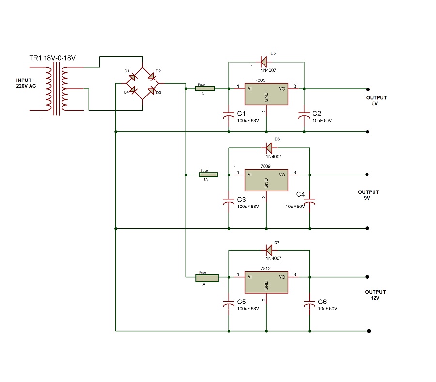
First of all, for stepping down the 230 V AC, an 18V-0-18V center tape transformer is taken. The secondary coil of the transformer is connected with a full-bridge rectifier. The full bridge rectifier is built by connecting four 1N4007 diodes to each other designated as D1, D2, D3 and D4 in the schematics. The cathode of D1 and anode of D2 is connected to one of the secondary coil and cathode of D4 and anode of D3 is connected to the center tape of the secondary coil. The cathodes of D2 and D3 are connected from which one terminal is taken out from the output of rectifier and anodes of D1 and D4 are connected from which other terminal is taken out from the output from full-wave rectifier.
For 5V supply, a fuse of 1A is connected in series to the output of full-wave rectifier for protection from the AC supplies. A capacitor of 100 uF (shown as C1 in schematics) is connected between the output terminals of the full-wave rectifier for smoothing purpose. For voltage regulation LM-7805 IC is connected parallel to the smoothing capacitor. The output is drawn from the voltage output terminal of the 7805 IC. A capacitor of 10 uF (shown as C2 in schematics) is connected across the output of the supply to compensate transient currents.
For 9V supply, again a fuse of 1A is connected in series to the output of full-wave rectifier for protection from the AC supplies. A capacitor of 100 uF (shown as C3 in schematics) is connected between the output terminals of the full-wave rectifier for smoothing purpose. For voltage regulation LM-7809 IC is connected parallel to the smoothing capacitor. The output is drawn from the voltage output terminal of the 7809 IC. A capacitor of 10 uF (shown as C4 in schematics) is connected across the output of the supply to compensate transient currents.
Similarly for 12V supply, again a fuse of 1A is connected in series to the output of full-wave rectifier for protection from the AC supplies. A capacitor of 100 uF (shown as C5 in schematics) is connected between the output terminals of the full-wave rectifier for smoothing purpose. For voltage regulation LM-7812 IC is connected parallel to the smoothing capacitor. The output is drawn from the voltage output terminal of the 7812 IC. A capacitor of 10 uF (shown as C6 in schematics) is connected across the output of the supply to compensate transient currents.
How the circuit works –
The power circuit operates in well-defined stages with each stage serving a specific purpose. The circuit operates in the following stages –
1. AC to AC Conversion
2. AC to DC Conversion – Full Wave Rectification
3. Smoothing
4. Voltage Regulation
AC to AC conversion
The voltage of Main Supplies is approximately 220-230V AC which needs to be stepped down to 12V level. To reduce the 220V AC to 12V AC, a step-down transformer with center taping is used. The use of center tap transformer allows to generate both positive and negative voltage at the input, however, only positive voltage will be drawn from the transformer. The circuit takes some drop in the output voltage due to resistive loss. Therefore a transformer of high voltage rating greater than the required 12 V needs to be taken. The transformer should provide 1A current at the output. The most suitable step-down transformer that meets the mentioned voltage and current requirements is 18V-0-18V/2A. This transformer step downs the main line voltage to +/-18V AC, as shown in the below image.

Fig. 3: Circuit Diagram of 18-0-18V Transformer
AC to DC conversion – Full Wave Rectification
The stepped down AC voltage needs to be converted to DC voltage through rectification. The rectification is the process of converting AC voltage to DC voltage. There are two ways to convert an AC signal to the DC one. One is half wave rectification and another is full wave rectification. In this circuit, a full-wave bridge rectifier is used for converting the 36V AC to 36V DC. The full wave rectification is more efficient than half wave rectification since it provides complete use of both the negative and positive sides of AC signal. In full wave bridge rectifier configuration, four diodes are connected in such a way that current flows through them in only one direction resulting in a DC signal at the output. During full wave rectification, at a time two diodes become forward biased and another two diodes get reverse biased.

Fig. 4: Circuit Diagram of Full Wave Rectifier
During the positive half cycle of the supply, diodes D2 and D4 conduct in series while diodes D1 and D3 are reverse biased and the current flows through the output terminal passing through D2, output terminal and the D4. During the negative half cycle of the supply, diodes D1 and D3 conduct in series, but diodes D1 and D2 are reverse biased and the current flows through D3, output terminal and the D1. The direction of current both ways through the output terminal in both conditions remain the same.

Fig. 5: Circuit Diagram showing positive cycle of Full Wave Rectifier

Fig. 6: Circuit Diagram showing negative cycle of Full Wave Rectifier
The 1N4007 diodes are chosen to build the full wave rectifier because they have the maximum (average) forward current rating of 1A and in reverse biased condition, they can sustain peak inverse voltage up to 1000V. That is why 1N4007 diodes are used in this project for full wave rectification.
Smoothing
Smoothing is the process of filtering the DC signal by using a capacitor. The output of the full-wave rectifier is not a steady DC voltage. The output of the rectifier has double the frequency of main supplies but contains ripples. Therefore, it needs to be smoothed by connecting a capacitor in parallel to the output of full wave rectifier. The capacitor charges and discharges during a cycle giving a steady DC voltage as the output. So, capacitors of 100 uF (shown as C1, C3, and C5 in schematics) are connected to the output of rectifier circuit. As the DC which is to be rectified by the rectifier circuit has many AC spikes and unwanted ripples, so to reduce these spikes capacitor is used. These capacitors act as a filtering capacitor which bypasses all the AC through them to the ground. At the output, the mean DC voltage left is smoother and ripple free.

Fig. 7: Circuit Diagram of Smoothing Capacitor for Triple Bench Power Supply
Voltage Regulation
The output voltages are drawn from the three regulator ICs. For taking three different voltages at the output three regulators are used. The 5V output is taken from the 7805 IC, the 9V is taken from the 7809 IC and 12V is taken from 7812 IC at the output. These ICs provide a constant and regulated output voltage. Hence any fluctuation and unwanted spikes in the input voltage do not affect the output voltage.
The 7805 IC provides an output voltage in the range of 4.75V to 5.25V with the input voltage range of 7V to 20V. The 7809 IC provides an output voltage in the range of 8.6V to 9.4V with the input voltage range of 11.5V to 24V. The LM7812 IC can have input voltages from 14.5V to 27V and it provides a constant output voltage from 11.4V to 12.6V. The ICs have maximum 1A current limit.

Fig. 8: Table listing input and output voltage of 7805, 7809 and 7812 Voltage Regulator ICs
These ICs have the following internally tolerable power dissipation –
Pout = (Maximum operating temperature of IC)/ (Thermal Resistance, Junction−to−Ambient + Thermal Resistance, Junction−to−case)
Pout = (125) / (65+5) (values as per the datasheet)
Pout = 1.78W
Therefore, 7805, 7809 and 7812 can internally sustain up to 1.78W power dissipation. Above 1.78W, these ICs will not tolerate the amount of heat generated and will start burning. This can cause a serious fire hazard also. So heat sink is needed to dissipate the excessive heat from the ICs.
Compensating Transient Currents
At the output terminals of the power circuit, 10 uF capacitors ( shown as C2, C4, and C6 in schematics) are connected in parallel. These capacitors help in fast response to load transients. Whenever the output load current changes then there is an initial shortage of current, which can be fulfilled by these output capacitors.
The output current variation can be calculated by
Output current ,Iout = C (dV/dt) where
dV = Maximum allowable voltage deviation
dt = Transient response time
Considering dv = 100mV
dt = 100us
In this circuit, a capacitor of 10 uF is used so,
C = 10uF
Iout = 10u (0.1/100u)
Iout = 10mA
This way it can be concluded that output capacitor will respond for 10mA current change for a transient response time of 100 us.

Fig. 9: Circuit Diagram of Transient Current Compensator
Short Circuit Protection
The diodes D5, D6, and D7 are connected between the voltage input and voltage output terminals of 7805, 7809 and 7812 ICs respectively, so that they can prevent the external capacitors (C2, C4 and C6 respectively) from discharging through the respective ICs during an input short circuit. When the input is shorted then the cathode of the diode is at ground potential. The anode terminal of the diode is at high voltage since the respective capacitor is fully charged. Therefore in such a case, the diode is forward biased and all the discharging current from capacitor passes through the diode to the ground. This saves the respective regulator IC from the back current.

Fig. 10: Circuit Diagram of Short Circuit Protection for Triple Bench Power Supply
Testing and Precautions –
The following precautions should be taken while assembling the circuit –
• The current rating of the step-down transformer, bridge diodes and voltage regulator ICs must be greater than or equal to the required current at the output. Otherwise, it will be unable to supply the required current at the output.
• The voltage rating of the step-down transformer should be greater than the maximum required output voltage. This is due to the fact that, the 7805, 7809 and 7812 ICs take voltage drop of around 2 to 3 V. Thus input voltage must be 2V to 3V greater than the maximum output voltage and should be in the limit of the input voltage of regulator ICs.
• The capacitors used in the circuit must be of higher voltage rating than the input voltage. Otherwise, the capacitors will start leaking the current due to the excess voltage at their plates and will burst out.
• A capacitor should be used at the output of rectifier so that it can handle unwanted mains noise. Similarly, use of a capacitor at the output of the regulator is recommended for handling fast transient changes and noise at the output. The value of output capacitor depends on the deviation in the voltage, current variations and transient response time of the capacitor.
• The protection diode should always be used while using capacitor after a voltage regulator IC, for preventing the IC from back current while discharging of the capacitor.
• For driving the high load at the output, heat sink should be mounted at the holes of the regulator. This will prevent the IC from blowing off due to heat dissipation.
• As the regulator ICs can draw current up to 1A only, a fuse of 1A needs to be connected. This fuse will limit the current in the regulator up to 1A. For current above 1A, the fuse will blow off and this will cut the input supply from the circuit. This will protect the circuit and regulator ICs from current greater than 1A.
Once the circuit is assembled, it can be tested using a multimeter. Measure the output voltage at the terminals of 7805 7809 and 7812 ICs. Then, measure the voltage outputs when loads are connected.
At 7805 regulator IC, the input voltage is 12V and the output voltage is 5.06V. With a load of 5 Ω resistance, the output voltage is read 3.43 V showing a voltage drop of 1.63 V. The output current is measured 590 mA. With a load of 10 Ω resistance, the output voltage is read 4.08 V showing a voltage drop of 0.98 V. The output current is measured 370 mA. so the power dissipation at a load of 10 Ω resistance is as follows-
Pout = (Vin – Vout)*Iout
Pout = (18–4.08)*0.370
Pout = 5.2W
At 7809 regulator IC, the input voltage is 12V and the output voltage is 9.15V. With a load of 20 Ω resistance, the output voltage is read 8.18 V showing a voltage drop of 0.97 V. The output current is measured 400 mA. With a load of 10 Ω resistance, the output voltage is read 7.38 V showing a voltage drop of 1.77 V. The output current is measured 680 mA. so the power dissipation at a load of 20 Ω resistance is as follows-
Pout = (Vin – Vout)*Iout
Pout = (18 –8.18)*0.4
Pout = 3.9W
At 7812 regulator IC, the input voltage is 12V and the output voltage is 12.22V. With a load of 20 Ω resistance, the output voltage is read 10.86 V showing a voltage drop of 1.36 V. The output current is measured 490 mA. With a load of 10 Ω resistance, the output voltage is read 9.02 V showing a voltage drop of 3.2 V. The output current is measured 830 mA. so the power dissipation at a load of 20 Ω resistance is as follow –
Pout = (Vin – Vout)*Iout
Pout = (18 – 10.86)*0.490
Pout = 3.5W
During testing of the circuit, it was analyzed that when current demand increases at the output then the output voltage starts reducing. As the current demand increases, 7805, 7809 and 7812 ICs start heating up and ICs take more drop across them which reduce the output voltages. As from the above practical experience, power dissipation in the ICs is found greater than their internal tolerable limits. So it is recommended to use heat sinks to aid cooling the ICs and to increase the lifespan of these voltage regulator ICs.
The circuit designed in this project can be used as a regulated power supply and in place as standard power adaptors. It can be used to bias Integrated Chips that require differential voltages.
You may also like:


Circuit Diagrams
Project Video
Filed Under: Tutorials
Filed Under: Tutorials

Questions related to this article?
👉Ask and discuss on EDAboard.com and Electro-Tech-Online.com forums.
Tell Us What You Think!!
You must be logged in to post a comment.