There are 2 cut off frequencies for band pass filter.
1. upper cut off frequency (f1) – the frequency below which all the frequencies are passed
2. lower cut off frequency (f2) – all the frequencies above this frequency are passed
From this f1 and f2 we shall define following parameters which are designing parameters for band pass filter.

Fig.1: Screenshot listing different parameters for band pass filter
Based on Q we have two types of band pass filter
1. Wide band pass filter – with Q <10 it has wide flat response over range of frequencies. BW is more
2. Narrow band pass filter – with Q>10 it has sharp bell type response. BW is very less.
Wide band pass filter
It’s actually combination of LPF and HPF as shown in figure

Fig. 2: Overview of Wide Band Pass Filter
Here F2 > F1. So we have to design HPF with F1 and LPF with F2. Suppose we want to pass the band of frequencies between 2 KHz to 5 KHz. so F1 = 5000 Hz and F2 = 2000 Hz.
Designing HPF section
Step 1: assume the required value of capacitor. It should be less than 0.1 micro Farad. This is required for better frequency stability. Suppose we assume value C as 10 nF (nano farad)
Step 2: calculate the value of resistance from equation

Fig. 3: Screenshot of calculations required to find resistance of HPF in Wide Band Pass Filter
Fig. 4:
so our assumption for capacitance value as 10 nF is good (or OK). Otherwise if the calculated value of R is much less than 1 KOhm, we have to assume some other value of capacitor. Because the value of R should not be less than 1 K Ohm.
Step 3: choose required pass band gain. Suppose we take it as 2. So form equation
Af = 1 + (R2 / R1)
2 = 1 + (R2 / R1)
R2 / R1 = 1
R2 = R1
Fig. 5: Screenshot of calculations required to find resistance of HPF in Wide Band Pass Filter
Designing LPF section
Step 4: assume the required value of capacitor. Suppose we assume same value C as 10 nF
Step 5: calculate the value of resistance from equation

Fig. 6: Screenshot of calculations required to find resistance of LPF in Wide Band Pass Filter
This value is odd value of resistor. May not be available as fixed value. So we may use potentiometer of 4.7 K? and tune it to desire value.
Step 6: choose required pass band gain. If we take it as 2 then again
R2 = R1

Fig. 7: Screenshot of calculations required to find resistance of LPF in Wide Band Pass Filter
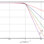
Final design with component values are as shown. Op-amp is active component and it requires +ve and -ve biasing voltages. One can test the circuit by applying input through signal generator and observing output on DSO or oscilloscope as well as bode plotter as shown in figure.

Fig. 8: Circuit Diagram of LM741 OPAMP IC based Wide Band Pass Filter
Note: – The schematic design is prepared in NI’s multisim 11 software. Software is available as free for 1 month trial period from NI’s website. Following all the circuits are also prepared in multisim 11 software.
Narrow Band Pass Filter
Step 1: for simplicity assume C1 = C2 = C
Step 2: select centre frequency fc = 2 KHz, pass band gain Af = 2, and Q = 10
Step 3: assume capacitor value C as 100nF
Step 4: calculate value of R1 from

Fig. 9: Screenshot of calculations required to find resistance for Narrow Band Pass Filter
Final design is as shown below.

Fig. 10: Circuit Diagram of LM741 OPAMP IC based Narrow Band Pass Filter
You may also like:
Project Video
Filed Under: Electronic Projects
Filed Under: Electronic Projects

Questions related to this article?
👉Ask and discuss on EDAboard.com and Electro-Tech-Online.com forums.
Tell Us What You Think!!
You must be logged in to post a comment.