An amplifier is a circuit which can produce an output voltage, which is the product of input voltage with a value called voltage gain. An op-amp (operational amplifier) is a kind of amplifier circuit which can perform an operation (addition, subtraction etc.) on the input voltages, apart from simply amplifying the input. It is an electronic circuit made of several active devices (transistors) and passive devices (resistor, capacitors) etc. which is capable of realizing following the common features:

History of op-amp Contd…


Basic functional blocks of an op-amp


Input Differential Amplifier Contd…


Output power amplifier

Fig. 12: Internal Circuit Diagram of 741 OPAMP IC
Op-amp symbol & Dual power supply
Op-amp symbol


Component significance
Fig. 16: Image of Regulated +/-5V Dual Supply
The above image is actually the dual power supply built by me. The circuit is exactly the same. The thing is that, I’ve built the circuit inside a switch box, with a power switch and plug point, so that it would be safe and easy to handle.
Features of 741 op-amp


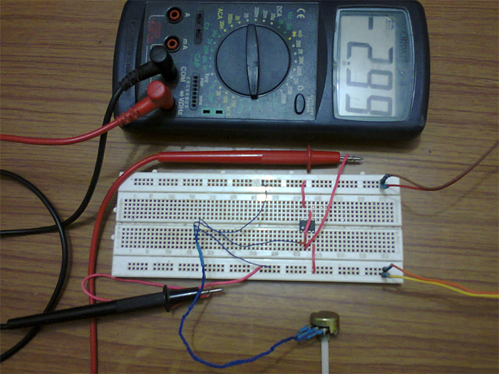
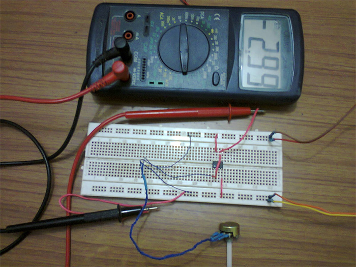
Testing a 741 IC


Testing a 741 IC Contd…


You may also like:


Filed Under: Featured Contributions, Tutorials

Questions related to this article?
👉Ask and discuss on Electro-Tech-Online.com and EDAboard.com forums.
Tell Us What You Think!!
You must be logged in to post a comment.