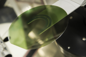
STMicroelectronics, a global semiconductor provider, announced that it has manufactured the first 200mm (8-inch) silicon-carbide (SiC) bulk wafers for prototyping next-generation power devices from its facility in Norrköping, Sweden.
 The transition to 200mm SiC wafers marks an important milestone in the capacity build-up for ST’s customer programs in automotive and industrial sectors.
It will further consolidate ST’s lead in the disruptive semiconductor technology that allows for smaller, lighter, and more efficient power electronics with a lower total cost of ownership.
Among the first in the world, ST’s initial 200mm SiC wafers are also high quality, with minimal yield-impacting and crystal-dislocation defects.
“The transition to 200mm SiC wafers will bring substantial advantages to our automotive and industrial customers as they accelerate the transition towards electrification of their systems and products”, said Marco Monti, president Automotive and Discrete Group, STMicroelectronics. “It’s important in driving economies of scale as product volumes ramp.”
A low defectivity has been achieved by building on the excellent know-how and expertise in SiC ingot growth technology developed by STMicroelectronics Silicon Carbide A.B. (formerly Norstel A.B., which ST acquired in 2019). In addition to meeting the quality challenge, the transition to 200mm SiC substrates requires a step forward in manufacturing equipment and the overall support ecosystem performance.
ST, in collaboration with technology partners covering the entire supply chain, is developing its own 200mm SiC manufacturing equipment and processes.
ST currently manufactures its high-volume STPOWER SiC products on two 150mm wafer lines in its fabs in Catania (Italy) and Ang Mo Kio (Singapore) while it performs assembly and test at its back-end sites in Shenzhen (China) and Bouskoura (Morocco).
This milestone comes as part of the company’s planned move to more advanced, cost-efficient 200mm SiC volume production. This transition is within the company’s ongoing plan to build a new SiC substrate plant and source over 40 percent of its SiC substrates internally by 2024.
“Building robust know-how in our internal SiC ecosystem across the full manufacturing chain, from high-quality SiC substrates to large-scale front and back-end production, boosts our flexibility, and allows us to better control the improvement of yield and quality of the wafers,” added Monti.
Filed Under: Automotive, Components, News, Products, Semiconductors


Questions related to this article?
👉Ask and discuss on EDAboard.com and Electro-Tech-Online.com forums.
Tell Us What You Think!!
You must be logged in to post a comment.